Visibility enhancement for full-chip simulation
The most expensive parts of today’s system-on-chip (SoC) design flow are where engineers must engage in direct manual effort or expend their energy making decisions. Unfortunately, far too much time and money are wasted on tasks that do not add value — such as trying to figure out if supposedly correct intellectual property (IP) is actually working, debugging ‘dumb’ errors, or deciding what signals to record in any given simulation run.
With small block-level simulation, it is fine to record every value change on every signal. This produces a rich database of time-ordered event data that can be used for understanding the design’s behavior and debugging errors. However, when the design gets very large, the overhead required to record all the events on all the signals overwhelms the run-time and fills the available disk space. Run-times can explode by a factor of five; disk requirements can run to the hundreds of gigabytes.
The extreme expense of recording all this data leads engineers to record too little information. The first simulation run is almost always executed without any recording at all. Engineers are optimists. So they simply run the design with the testbench checking for problems, not really expecting to find any. But the verification methodology breaks down when the testbench flags a mismatch between the expected results and the actual behavior. Now the team has to figure out what to dump — do they turn on full recording of every signal for the entire run, and risk filling the disks? Or do they selectively dump based on their best-guess of where the problem lies, and risk a third run in the case that they are wrong?
The lack of predictability in this process is a huge problem, particularly since full-chip simulation runs are often at the end of the verification cycle. Should the team build the chip, hoping the problem is not in the hardware? Or hold up the fab until it tracks down the cause of the mismatch? If it takes one day for the no-recording simulation, it will take five days for the full-dump pass. Or maybe it will take two days for a partial dump that may or may not have the data needed. What are the options?
New visibility enhancement technologies enable engineers to make intelligent tradeoffs between impact (simulation performance and file size) and observability. With lots of impact, it is easy to see everything. With no impact, nothing can be observed. The trick is to find a way to minimize impact while achieving full visibility — or at least enough visibility to effectively debug complex chip problems.
Visibility enhancement
Research by Novas Software has revealed that there are three steps which optimize our ability to debug a chip with minimal impact on observation:
- Analyze the design to determine which signals are essential for full visibility.
- Expand the limited data of the essential signals to obtain values for the rest of the design’s signals.
- Correlate the abstraction from which the signals were dumped back to the familiar RTL representation.
Formal analysis of an RTL description or netlist provides the engineer with a list of observable signals. Observation of the values of these signals over time enables full visibility within a designated portion of the design. Once the essential signals are dumped, additional analysis can fill in the blanks for the signals that were not dumped, making a full set of values over time available for debugging.
For full-chip RTL simulation, or for those few designers who are familiar with a netlist, essential signal analysis and data expansion may be adequate. Much of the challenge of late-stage debugging lies in understanding the workings of the actual chip or its detailed netlist — something that is unfamiliar to most engineers. Mapping the gate-level netlist signals up to the RTL level can alleviate this: the logic description is much more familiar and the level of abstraction aids comprehension of design behavior.
Visibility analysis
Visibility analysis technology analyzes assertion, RTL or netlist HDL code to decide what are the minimum essential signals needed for debug (Figure 1). This technique reduces the amount of data that needs to be dumped for full visibility, which, in turn, drastically reduces the size of the dump file and the overhead of dumping. As a result, verification turnaround time is substantially decreased.
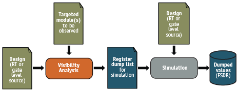
Figure 1. Visibility analysis determines which design registers should be dumped during simulation in order to minimize the impact on performance while maximizing signal observability
To determine the essential signals, visibility analysis relies on a complete set of logic equations inferred from the HDL description. For each functional block, it recursively traverses the inferred logic netlist and extracts the primary inputs, register outputs, memory outputs, and the outputs of non-synthesizable blocks. It then writes these signals into a file that can be used to control dumping by a simulator.
Visibility analysis can be applied in three areas: assertion, RTL/netlist and silicon debug.
For debugging assertion failures, it analyzes the design and the selected assertions to extract the minimal set of design signals needed to debug each assertion. By dumping just these signals and evaluating the assertions after simulation, overhead during simulation is reduced, the process is parallelized and overall turnaround time is improved.
For full-chip simulation, it analyzes the RTL or netlist code to find the storage elements, memory elements and primary inputs. Instead of dumping every signal in the design, it dumps only the essential signals. Full visibility can be achieved using data expansion technology.
Since the number of essential signals in a typical design is significantly smaller than the total number of signals, visibility analysis can reduce run-time on a simulation that might otherwise require an overnight run for a full dump to a couple of hours.
This technology can also be applied to in-situ silicon testing. Here it determines a minimum set of registers required to provide visibility for the portion of the design being exercised. This information provides useful guidance for the insertion of instrumentation logic.
Data expansion
Understanding abnormal device behavior is difficult when only a subset of data is available from the device. Data expansion technology can be applied to compute the missing data using knowledge of the design function. After the values of the missing signals are computed, debugging techniques that rely on signal information over time can be enabled to allow the tracing of causes from effects.
Given the values of registers and primary inputs, data expansion sorts the combinational logic between the registers using a linear ordering algorithm. It then computes the values for these signals using a cycle-based evaluation engine (logic and wire delays are not considered). The computed values are sent through a data agent to the application window(s) in which the user is exploring the design.
Novas’ expansion technology computes the values of signals ‘on the fly’: only the values of the signals required by the current operation or display are computed. To do this, a new value, Not Computed (NC), is introduced in the waveform database and display. When the value of a signal has not been dumped or expanded, the NC value is stored and displayed. After expansion, these signals appear normally, but are shown in a different color to differentiate them from dumped signals.
Abstraction correlation
A gate-level design view is typically hard to understand when generated by synthesis tools. To easily understand the meaning of gate-level logic, one needs the ability to correlate back to the RTL design, or even a system-level description. Due to synthesis and optimization, not every net of a gate design will have a corresponding signal in the RTL circuit. Nonetheless, it is useful to localize the region related to specific nets. To accomplish this, it is reasonable to assume that registers have one-to-one correspondence in typical applications. It is natural, therefore, to try mapping the registers first and then to use this information to localize net correspondence.
Abstract correlation technology solves this problem with the use of structural dependency graphs and approximate graph matching. Internal net matching via localization is also performed after the registers and essential signals are matched, albeit with more uncertainty due to the optimization introduced in synthesis. The idea of mapping using structural dependency graphs imitates the process of human debugging, in which one often locates the corresponding areas by looking at registers in the fan-in and fan-out cones.
Debugging at multiple levels using netlist signal data
By combining abstraction correlation and data expansion technologies, it is possible to debug the results from gate-level simulation in conjunction with the corresponding gate-level or RTL design source code. Novas’ on-the-fly expansion technique makes this practical, as there is no need to suffer the overhead of a complete mapping and expansion prior to debug. Instead, the signal mappings and data expansion are performed as needed during debug.
Full-chip simulation application
Full-chip simulation often requires a trade-off between performance and debug. Generally, a greater understanding of the behavior, and therefore quicker debug, is achieved by dumping as much signal data as possible. Unfortunately, a high amount of dumping significantly degrades simulation performance and produces enormous dump files. As a result, many verification teams avoid signal dumping in favor of iterating lengthy simulations. Signal dumping is utilized only after an error is discovered. The number of total iterations using this approach is not possible to predict and could significantly impact the design schedule.
Using a methodology that limits the dumping to a small but critical subset of signals, verification teams can achieve full-chip functional simulation debug with minimal performance impact. This methodology relies on the selection of a minimal number of dumped signals, yet provides observability of most signal values. The dumping can usually be limited to registers. If the desire is to limit the registers to monitor only a specific module, they must be carefully selected. Visibility analysis assists with the selection of registers to be included in the dump list to ensure visibility of the desired signals.
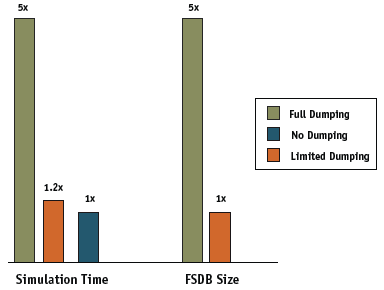
Figure 2. Visibility Enhancement Results. Simulation times and dump file sizes decrease using limited dumping and visibility enhancement technology
Prior to running simulation, the simulator is set to only dump the list of registers. After the simulation, the dumped data is processed with data expansion. Data expansion operates on the available data to compute the combinational node values on a cycle basis, without consideration of timing delays. By way of example, data expansion is invoked automatically on the fly during debug with the Verdi Automated Debug System from Novas. The resulting data is processed as if it had been dumped directly.
Using this register-limited dumping methodology, the verification team can immediately start debugging after discovering an error with the simulation results rather than waiting for long re-simulations with full dumping. This methodology enabled by data expansion allows high to full observability of the design with minimal impact on performance. The data to date shows that the resulting simulation is almost four times faster (1.2x compared to 5x) when compared to full dumping, and requires only minimal performance impact compared to no dumping (1.2x compared to 1x). It also shows the corresponding dumped FSDB file sizes are much smaller compared to those produced with full dumping (Figure 2). Specific results will vary according to factors such as design topology and distribution of simulation activity.
Conclusion
Visibility enhancement technology can mitigate the expense of obtaining enough signal value information to debug complex problems. By automatically analyzing a design to determine the essential signals, expanding the values for signals not dumped,
and correlating low-level signals back up to the RTL level, design comprehension is greatly enhanced and debug time is dramatically reduced, along with the cost of verification. While we have described in detail how visibility enhancement technology is applied to full-chip simulation, it is also particularly relevant for emulation and FPGA prototyping as well as in situ silicon validation.
Novas Software
2025 Gateway Place
Suite 400
San Jose
CA 95110
USA
T: 1-888-NOVAS-38 or +1 (408) 467-7888
https://www.synopsys.com/Tools/Verification/debug/Pages/siloti-ds.aspx
