Using self-timed interconnect to accelerate SoC timing closure
Timing closure is one of the major problems faced by SoC designers. The inclusion of several, often diverse, IP cores that need to communicate with each other on a chip makes it difficult for a designer to meet the complex timing requirements between these cores.
Furthermore, as process nodes shrink, process variability becomes a more important consideration, adding to the difficulty of designing a high-yielding chip that successfully meets its performance specifications.
The problems facing timing closure are exacerbated by clock tree balancing, clock skew and jitter, as well as low-power techniques, including clock-gating and numerous clock domains. Thus the issue becomes dramatically more difficult to overcome as the industry migrates to deeper and deeper submicron technology. While a synchronous (clock-based) chip-design methodology has served the semiconductor industry well in the past, it has run out of steam for today’s leading-edge SoC designs. It is time to look at self-timed (clock-less) interconnect as a way of overcoming the critical timing-closure problem.
This paper will describe the problems associated with clockbased SoC design and show how eliminating a global clock and using a self-timed interconnect fabric significantly shortens timing closure – along with offering several other benefits – while reducing a chip’s time-to-market. Included in the discussion are reasons why self-timed circuits, which have been around for several decades, have taken so long to catch on and how the adoption of this design methodology requires the right types of design tools for composing, analyzing and synthesizing self-timed interconnect fabrics.
Clocked vs. self-timed chip networks
As system-on-a-chip (SoC) complexity continues to climb and process nodes shrink, the overall task of designing a chip that meets its performance specifications becomes more difficult. One the most challenging tasks facing the chip designer is timing closure – making sure critical timing-path delays that were estimated during the logic portion of the design match the extracted delays from the chip’s layout. Several trends in the semiconductor industry are making this job harder today:
- As process nodes shrink, interconnect delay becomes an increasing percentage of the total delay between two points on the chip (wires remain long, but get thinner and narrower). Furthermore, process variability means that RC wire-delay variability becomes a larger percentage of nominal wire delay as chips are fabricated with smaller features.
- As SoCs are comprised of a larger number of more complex IP cores, the task of coordinating the timing requirements of these cores synchronized with a single clock across the entire chip becomes even more difficult.
- The move towards multiple clock domains on a chip, done mainly to reduce power dissipation, exacerbates the timingclosure problem and generally increases latency and decreases overall traffic throughput.
With a synchronous clock-based digital design, the global clock signal provides ‘traffic control’ as data is stored, processed or transferred between the various circuits on the chip. The SoC comprises many subsystems, each often with its own clock domain. This requires a global clock, along with buffers and synchronizers to maintain data integrity and manage metastability between the separate clock domains. The presence of a global clock, while simplifying overall SoC design, typically adds approximately 30% area and power overhead.
A traditional clock-based bus interconnect scheme for synchronizing total chip operation is very difficult to design due to the trends previously discussed and to the inaccuracy of the models for the IP on the chip. Even a well designed global clock network has some amount of skew. For example, for a 400MHz clock an acceptable 5% skew amounts to 125ps. To account for this skew and the normal fluctuations in chip performance caused by process, temperature and voltage variations, a designer has to work with some amount of design margin – the smaller the margin, the better the results but the harder it is to reach timing closure. Many SoCs now have multiple buses, each with its own protocol, and with bridges between them, making the problem of reaching timing closure for the chip even more difficult. Increasing the clock frequency is not the answer; this just introduces additional problems for the designer.
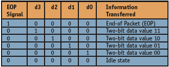
Figure 1. One-of-five data encoding
As an alternative to traditional clock-based bus architectures, self-timed on-chip networks eliminate the need for a global clock. Communication between blocks, instead of being controlled by a clock signal at fixed clock edges, is done with a handshaking scheme. One way of achieving a self-timed network that does not require delay-path matching is delay-insensitive data encoding (i.e., encoding that is tolerant of propagation delays in wires and logic) coupled with a return-to-zero signaling protocol on interconnect links with one acknowledge wire and five forward-going wires. This one-of-five data encoding results in six wires per link, with only one wire allowed to signal data at any time (one-hot encoding)1.
As shown in Figure 1, one of the d0-d3 wires transmits two bits per baud during data transmission. The EOP signal separates data blocks. This encoding scheme uses a five-input NOR gate to detect valid data and you can use multiple parallel links if you need higher bandwidth between two endpoints. This self-timed interconnect scheme also uses low-latency transparent pipeline latches instead of buffers on long links. This improves the bandwidth of these links without adding significant latency as flip-flops would in synchronous buses.
Several data-wire groups can share the EOP and acknowledge signal and the wire ‘cost’ for this self-timed approach for a data path n-bits wide is 2n + 2 wires, n/2 2n-input OR gates, and an n/2-input Muller C-element tree2. By decoupling the IP cores on an SoC, a self-timed interconnect fabric eliminates the design difficulty associated with long clock lines and also reduces clock jitter and noise problems. Each IP core can run at its own ‘best’ frequency and the clocking rates of the individual cores do not have to be derivatives of a ‘master clock’. The speed of data along the self-timed interconnect links is limited by the wire speed and not by a global clock. Consider the comparison shown in Figure 2. For the synchronous bus architecture on the left, each color represents a different clock domain. Every clock must be a derivative of a master clock and timing closure is very difficult. The self-timed interconnect on the right replaces the rigid bus hierarchy with an interconnect topology that is tuned for the performance goals of that particular design.
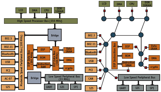
Figure 2. Comparsion of synchronous bus (left) and self-timed interconnect architectures
Developing a flexible self-timed interconnect fabric
You can implement a self-timed interconnect fabric for an SoC using a fixed topology, such as a crossbar switch or tree network. However, this ‘one size fits all’ approach does not allow designers to choose the best IP connection scheme for their particular design. A better idea is to investigate different topologies at a high abstraction level, analyze the performance of each, and then synthesize the best one. This requires a set of specialized EDA tools for exploring and synthesizing circuit-specific interconnect fabrics (Figure 3).
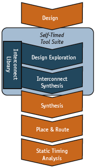
Figure 3. EDA tools for exploring and synthesizing circuit-specific interconnect fabrics
First is a graphics-based design exploration tool that allows the designer to do ‘what if ’ analyses of different self-timed interconnect topologies. The tool should generate the correct models for both high-level (SystemC) and Verilog functional simulations. Next is a tool that will synthesize the interconnect wires along with all the self-timed interconnect elements needed to produce the fabric and have it communicate with the various elements of clock-based IP on a chip. Standard logic synthesis tools cannot handle the logic of the various gateways, synchronizers and de-synchronizers. Designers need a specialized synthesis tool to produce a structural netlist of the self-timed fabric, working like a pre-compiler prior to regular logic synthesis.
Finally, the tool suite must include access to a library that contains the various components that the self-timed interconnect fabric uses.
Benefits beyond simplifying timing closure
Along with faster timing closure, self-timed chips offer several other advantages for the designer. Such circuits demonstrate significantly lower dynamic power dissipation than do bus-based synchronous chips. This is because power in the interconnect, which is a significant portion of total chip power, is only dissipated when data is being transferred between endpoints and is not clockdependent. With clock-based interconnect, power is dissipated on every clock edge, whether or not data is moving.
The performance of self-timed chips is also better since you do not have to add design margins to account for clocking issues. The clock speed for a synchronous chip is based on the slowest path on the chip, analogous to the weakest link in a chain. Data for faster circuits must be delayed until the slowest data path completes data transfer. For a self-timed chip, the data-transfer speed is close to the average data rate for all circuits on the chip. Each interconnect path will work at a speed limited only by wire delays, not dictated by the necessity of meeting setup and hold times for the individual IP blocks.
Self-timed chips also are less noisy than synchronous chips, again due to the lack of a global clock that generates noise spikes at every clock transition. This also results in less electromagnetic interference (EMI) for self-timed chips. Since logic transitions between cores occur at broad intervals, the EM energy they produce is spread throughout the frequency spectrum. On the other hand, clock-based chips produce large amounts of EM energy at the clock frequency and its harmonics.
Finally, eliminating the global clock for a self-timed chip significantly reduces the time needed to lay out the chip, since clock-tree generation and verification are very time consuming.
References
- J. Bainbridge and S. Furber, “CHAIN: A Delay-Insensitive Chip Area Interconnect”, IEEE Micro, V22, No. 5, Sept./Oct. 2002, pp. 16-23.
- I. Sutherland, J. Ebergen, “Computers without Clocks”, Scientific American, August 2002.
Silistix
101 Metro Drive
Suite 335
San Jose
CA 95110
USA
T: 1-408-878-6098
F: 1-408-878-6100
W: www.silistix.com
