Using multi-corner multi-mode techniques to meet the P&R challenges at 65 nm and below
Concurrent multi-corner, multi-mode analysis and optimization is becoming increasingly necessary for sub-65nm designs. Traditional P&R tools force the designers to pick one or two mode corner scenarios due to inherent architectural limitations.
As an example of the problem, a cellphone chip typically needs to be designed for 20 mode/corners scenarios. In the absence of a implementation system that can handle multiple mode/corners scenarios simultaneously, the design team has to implement the design for a chosen worst corner, set some margins/pessimism, and then hope that the chip works at other mode/corners. The verification process includes extraction and timing runs for each mode/corner separately followed by blind non-convergent ECO loops where a fix at one mode/corner can break it at another. A further complication is that such analysis is often left until the end of the design flow, and any ECOs that arise therefore place even greater pressure on project schedules.
The paper describes an alternative strategy that uses a new analysis data-model to give concurrent access to all scenarios, and which ensures that access is more evenly distributed across the design process.
As nanometer geometries move into the 65nm and 45nm realms, variability is rapidly becoming one of the main causes of chip failures and delayed schedules. Discontinuities such as process variation, design size, low power and design-for-manufacture (DFM) have created a major disruption in the physical design process with regards to advanced ICs for cutting-edge wireless, handheld, processor, graphics, set-top box, and networking applications. This article discusses how variability affects today’s flows and how to address it.
Failures, missed windows, and outdated flows
At 65nm, 45nm and below, designers are forced to juggle the challenge of controlling macro-level functional complexity issues (operational modes) with micro-level process issues (corners), all while trying to meet ever-tightening silicon delivery targets. The problems raised by multiple chip operating contexts and process variations have been addressed through painful constraint mergers, and guesses as to the design margins and worst-case corner conditions, made during the early phases of the design cycle.

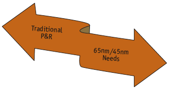
Figure 1. Inherent tensions below 65nm
During the cycle’s later phases, such outdated implementation flows force designers to manually analyze and fix the effects of all other design and process variation combinations in an iterative and non-convergent way. More proactive management of design and process variations across the entire flow is critically needed to reduce the likelihood of chip failures. Such an approach is variously referred to as design-for-variability (DFV) or multi-corner multimode (MCMM) design. In the absence of such capabilities, designers face unpredictable iterations during the sign-off ECO loop, and must factor in pessimistic margins that produce designs with reduced performance, larger area and power dissipation, and lower yields.
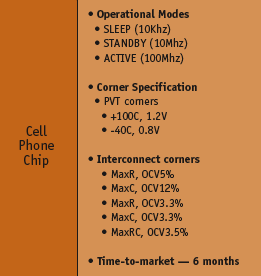
Variability has always been a concern, but at 65nm and 45nm it is growing the number of corner cases and modes. This, in turn, significantly complicates the physical design task. For example, a cellphone chip must have three different modes of operation, and satisfy two PVT corners and five interconnect corners (Figure 2).
Consequently, the physical layout and verification must take into account 20 different mode/corner scenarios to meet all the constraints imposed by the different modes of operation with process and manufacturing variation (modeled by the corners). Despite all this complexity, the chip must be completed in six months or less to meet stringent market demands.

Figure 2. Modes and corners for a cellphone chip
By contrast, established physical design flows can handle at most one or two scenarios at a time. So designers must choose between either limiting the number of modes and corner cases or devoting weeks to running multiple extraction/timing analyses followed by painful ECOs. Given time-to-market pressures, design teams usually choose the first option, a severely limited corner/mode scenario that combines the worst-case parameters. A typical two-corner analysis consists of:
- Late (setup) analysis at weak, minimum voltage, high temperature conditions.
- Early (hold) analysis at strong, maximum voltage, low temperature conditions.
Nominal interconnect models are generally employed and some margin is used to cover up uncertainty. This approach is obviously less than ideal. First, it provides no guarantee of convergence, since optimizing a timing path in one scenario can cause a new violation in a different one. Moreover, in the case of a mobile phone chip, each iteration will be accompanied by five RC extraction and 20 timing analysis runs. This clearly increases the engineering effort during the already stressful final stages of any chip implementation. It can hardly come as a surprise that taking this limited approach, coupled with late-stage unpredictability, has resulted in a higher rate of chip failures and more delayed or missed project deadlines.
An architecture to address variations natively
Analyzing and optimizing variability
To truly optimize a design for variability and minimize yield loss, one must electrically model deterministic variability with analysis and implementation tools. Interconnect variation under conditions from those of maximum resistance (i.e., minimum cross section area) to those of maximum capacitance (i.e., maximum cross section area), and everything in-between must be considered. Similarly, the analysis infrastructure must be robust enough to handle device effects such as temperature inversion, negative bias temperature instability (NBTI) and pin capacitance variations.
Operational variability, such as standby modes, should be addressed by performing simultaneous analysis of multiple design modes. The physical design environment should accept mode-specific timing constraints and the analysis should be performed without mixing data across different modes. Global variability should be addressed by performing simultaneous analysis across multiple analysis corners. An analysis corner reflects a particular global operating condition (PVT), and corresponds to a set of characterized device and interconnect libraries. It can be configured for various analysis objectives such as setup, hold, noise and so on.
Local variability should be analyzed in the context of global variables by modeling them as variations around a corner. Some sources of local environmental variability, such as IR drop and crosstalk, can be directly analyzed; others, such as NBTI, can be analyzed by specifying two variation libraries around a corner. Local manufacturing variability in the interconnect can be addressed by using selective process bias around a corner. Device threshold voltage (VT) variations due to local manufacturing variability can be analyzed either by using ‘min/max’ variation libraries around a corner or by using linear delay derating.
Concurrent analysis over MCMM scenarios
Since the goal of design for variability is to generate a single circuit implementation that satisfies the constraints of different variation scenarios, concurrent analysis over all these scenarios is necessary. As mentioned earlier, traditional tools limit the analysis runs to at most two scenarios, possibly one. So, a design with 64 different scenarios requires anywhere from 32 to 64 runs, and the team must then laboriously scrutinize the report files to determine if there are problems that need to be fixed.
Mentor Graphics’ next-generation analysis system, Olympus-SoC, can concurrently analyze all the scenarios in one shot (i.e., one timing analysis trace), allowing the user to quickly narrow down any probable violations, greatly improving engineering productivity and reducing human error. It is capable of representing multiple variation scenarios in memory concurrently.
To address the issue of scalability, the flow employs a new analysis data-model that takes advantage of data duplication across the different variation scenarios and stores the concurrent timing graph for these in a very compact fashion. That way, designers always have access to all violations over all variation scenarios at every stage during implementation. This completely eliminates the unpredictable and costly iterations that happen at the very end of design projects in current-generation flows.
Concurrent optimization: ‘one-shot’ eliminates iterations
With the ability to analyze variations over all scenarios, the next logical step is to optimize the design to meet all its variation constraints. The optimization engine in Olympus-SoC is capable of performing concurrent ‘N corner’ optimization without needing any simplification or reduction. Multiple setup corners and multiple hold corners can be concurrently analyzed and optimized. The ability to perform N corner optimization significantly simplifies several cumbersome design variation applications such as dynamic voltage frequency scaling (DVFS), hold optimization and leakage optimization.
For example, one of the biggest challenges in design variation is clock tree synthesis. With the proliferation of increasingly sophisticated mobile devices, clock trees have become extremely complex circuits with different clock tracing for each circuit mode of operation. Furthermore, building robust clock trees that can withstand process variation is a big challenge. If you can perform concurrent N corner analysis, the clock tree synthesis challenge can be addressed head-on. Clock-tree construction can measure early and late clock network delays over all process corners concurrently, accounting for both global and local variation. Design teams can check and adjust clock skew and latency over all process corners ensuring a robust clock tree.
Handling MCMM Designs
Dealing with escalating variability in physical design is a reality that engineers face when working with nanometer technologies. Existing design technologies do not include sufficient resources to adequately address multiple modes and multiple corner cases in an efficient, comprehensive manner. Fortunately, a new strategy and tool chain now exists to address the problem of concurrent analysis and implementation over a number of design variation scenarios in a scalable fashion.
Sources of variability
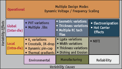
Variability in 65nm and 45nm ICs stems from three major sources, summarized here and in Figure 3. Operational design variation refers to different operating modes of a chip. For example, a mobile phone chip is required to work in ‘sleep’, ‘standby’ and ’active’ modes. Different modes come with different design constraints that must be simultaneously analyzed for fast design closure.

Causes and effects of variability
Global design variation is the difference in the value of a parameter across nominally identical die (whether those die are fabricated on the same wafer, on different wafers, in different lots, or in different fabrication plants) and is typically accounted for in circuit design as a shift in the mean of some parameter value equally across all devices and structures on any chip.
- Global environmental variations such as ambient temperature and supply voltage can change the electrical characteristics of devices. Worst-case timing has been traditionally modeled using low voltage, slow process and high temperature. Nanometer technologies have started to exhibit inverted temperature behavior whereby worst timing is achieved at low voltage, slow process and low temperature. The temperature inversion effect varies for each library cell on a timing arc basis and gets worse when lower operating voltages are used.
- Global manufacturing variations include geometric and material parameter variations in the device and the interconnect. Geometric variations such as effective ‘channel length’ variation and ‘film thickness’ variation can result in systematic chip-to-chip threshold voltage (VT) and leakage current variations. Similarly, deviations in the width of lower metal layers due to proximity and lithographic effects can directly impact line resistance as well as coupling capacitance. Global variation in metal and dielectric thickness also leads to global resistance and capacitance variations.
Local design variation is the deviation occurring spatially within any one chip. Such intra-chip variation may have a variety of sources depending on the physics of the manufacturing steps that determine the parameter of interest. It is once again caused by environmental and manufacturing variations.
- Local environmental variations are caused by operation of the chip and include local effects such as device voltage variations due to IR drop and ground bounce; delay and slew variations due to crosstalk; input pin capacitance variation due to slew and state dependency; and device performance degradation due to negative bias thermal instability.
- Local manufacturing variations include device and interconnect geometry variations due to local layout as well as random material parameter variation. Interconnect line width and spacing deviations arise primarily due to photolithographic and etch dependencies. These deviations directly impact interconnect parasitics and result in performance and signal integrity degradation. Significant local metal thickness variation has been observed for copper interconnect layers resulting in dishing and erosion. Similarly chemical mechanical planarization (CMP) can introduce strong dielectric thickness variations across the die.
Mentor Graphics
Corporate Office
8005 SW Boeckman Rd
Wilsonville
OR 97070
USA
T: +1 800 547 3000
W: www.mentor.com


