The USB 3.0 Physical Layer
A look at the USB 3.0 physical layer, including the PHY and the physical connection between two ports, which is carried on two differential data pairs.
<= Previous article: USB 3.0 Link Layer
The Physical Layer represents the PHY and the actual physical connection between two ports. The physical portion of the link represents the two differential data pairs: one transmit path and one receive path.
The Physical Layer receives the 8bit data from the link layer, scrambles it to reduce EMI, encodes the scrambled data into 10bit symbols, and serializes the data to be sent over the cable. At the receiving end, the reverse operation is performed.
The transmitter functions of the Physical Layer include data scrambling, 8b10b encoding, and serialization.
The receiver functions of the Physical Layer include de-serialization, 8b10b decoding, data descrambling, and receiver clock and data recovery.
In practical terms, the Link Layer contains the media access layer including state machines for link training, flow control and status. This is connected, via the PHY/MAC interface, to Physical Layer functions such as the physical coding sub-layer, which handles the 8b10b encoding/decoding, buffering and receiver detection, and the physical media attachment layer, which includes a 10bit interface, SerDes and analog buffers.
The interface between the PHY and the MAC is known as the PIPE interface. The data crossing the interface can be 8, 16 or 32bit wide. A PCLK is recovered from an incoming connection and passed from the PHY to the MAC. There are also signals on the PIPE interface to indicate whether what is on the data bus is real data or special symbols; 12 or 16bit command signals to control the PHY layer; or other status signals.
The PIPE interface also handles the low-frequency periodic signalling that is used when both sides of the link are in a low-power state, to ensure that one side of the link can still wake up the other side of the link. This means that the PHY can be put into a very low-power state, running only the circuitry necessary to recognise and respond to the low-frequency periodic signalling.
In terms of electrical signals, a USB 2.0 PHY launches an 800mV peak-to-peak signal into a cable but suffers poor signal integrity (at its highest operating speed of 480Mbit/s) due to reflections. The eye at the receiver is usually about 400mV peak-to-peak and 1.5ns wide.
A USB 3.0 PHY launches a 1,000mV peak-to-peak signal, which translates to a 600mV peak-to-peak signal without a USB 3.0 cable present, and a 500mV peak-to-peak signal at the far end of a USB 3.0 cable. The eye opening is very small – just 100mV peak-to-peak and less than 100ps wide.
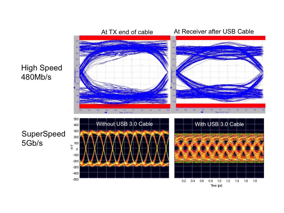
Figure 1 The eye opening in a USB 3.0 signal is much smaller than that in a USB 2.0 signal (Source: Synopsys)
To deal with the frequency-dependent losses of a USB 3.0 signal, equalisers are applied at both the transmit and receive ends of the link. The USB 3.0 specification requires a 3.5dB transmit equaliser and a 6dB receive equaliser. [The receive equaliser can be designed to be adaptive if necessary.]
The Physical Layer also has to contend with the fact that there is no shared clock signal between the transmitter and receiver: only data crosses the link. The USB 3.0 specification also requires a spread-spectrum clock, that is one whose frequency varies by up to 5000ppm at 33KHz to reduce the EMI impact on the cable ground. This means that USB 3.0 receivers are constantly ‘chasing’ the clock to get a lock on it. The situation is eased by encoding each 8bit byte that crosses a USB 3.0 interface in 10 bits, to introduce more signal transitions, which helps with clock and data recovery. Other techniques are used to help word alignment and error detection.
Further information
If you are new to designing with USB, or looking for tips on implementing USB 3.0 IP, attend Synopsys’ “USB 3.0 University.” Topics in this instructional video series range from fuller descriptions of the USB 3.0 Physical Layer and more. Click on the links below.
USB 3.0 Protocol Layer – Part 1
USB 3.0 Protocol Layer – Part 2
Company info
Synopsys Corporate Headquarters 700 East Middlefield Road Mountain View, CA 94043 (650) 584-5000 (800) 541-7737 www.synopsys.comSign up for more
If this was useful to you, why not make sure you’re getting our regular digests of Tech Design Forum’s technical content? Register and receive our newsletter free.
