The three critical data validation points in a design flow
Why design data integrity matters from cell design to tapeout. These techniques will help ensure your validation process is as comprehensive as possible.
Companies that develop integrated circuits (IC) typically build semi-custom design flows for their internal design teams to ensure the final manufactured products meet all requirements and can be delivered on schedule. Foundry support teams provide the physical verification rule decks, manufacturing requirements, technology files, and design kits that internal teams use to ensure manufacturing compliance, while the flow designers strive to streamline processes to maximize design throughput.
Many design teams are composed of globally-dispersed members who frequently work in close collaboration using parallel design implementation flows. However, while parallelizing implementation is one way to meet aggressive schedules, mistakes made by any one group will likely impact others. Incorrect data provided after design iterations or format translations is often a recurring source of such issues. To minimize this possibility, flow designers add physical design data validation checks throughout to validate the design data, specifically targeting a comparison of two input databases. These validation checks typically utilize geometric XOR and NOT operations, with the results either validating a particular step in the flow, or identifying an error that should be resolved before continuing. While these types of validation flows are highly recommended, they can be eat up a lot of runtime and resources when run on very large designs, and are not particularly well-suited to some data comparison flows.
Layout data integrity and the design flow
Physical design data is most commonly shared in GDSII or OASIS formats, but can also be provided in OpenAccess, LEF, DEF, or proprietary database formats, as required for input or output from the design tools used throughout the flow.
Unintended changes can be introduced when a designer or computer-aided design (CAD) engineer converts design data from one format to another, or merges data from two databases. For example, accurately exporting design data from an OpenAccess database to GDS requires that designers first draw layout objects correctly, and then map them to GDS with a mapping file. Objects drawn on incorrect layers, or not properly specified in the map file, can contribute to issues in downstream flows. Moreover, merging a GDS design with fill objects or other design-for-manufacturing (DFM) enhancements may create errors due to incorrect mapping, or actually result in dropped data if cell names are in conflict between the input databases.
Hard IP libraries like standard cells, memories, or pad cells are typically distributed with GDS, OASIS, and LEF abstract format representations. The GDS or OASIS cells are included in the final design taped out to the foundry, while the LEF abstracts – containing standard cell footprints, pin names, pin locations, and routing blockages – are required for place and route (P&R) flows. Because these libraries are usually purchased from third parties or delivered by specialized design groups, it is reasonable to assume that the contents for each data format are consistent with and correct across all formats.
On the other hand, the size, pin location, obstructions, or power grid for soft IP developed internally must be determined during the design process, relative to design considerations such as available space in the chip-level floorplan, pin-out requirements, routing limitations, and top-level power grid. Throughout the course of a project, these details may change, as dictated by the chip-level design team or the block implementation team. Due to the often-dynamic nature of the integration of these soft IP blocks, the GDS, OASIS, and LEF versions can fall out-of-sync between teams. In addition, internally-developed soft IP may be created in OpenAccess, then converted to GDS, OASIS, and LEF formats. Any errors in these conversions can lead to discrepancies between the various formats.
Design data represented as cells and blocks developed and referenced throughout the design flow go through multiple iterations before reaching tapeout (Figure 1). Each iteration may result in design data slipping out of sync. Building in reasonable data integrity checks in a design flow can help ensure correct versions are referenced at tapeout.
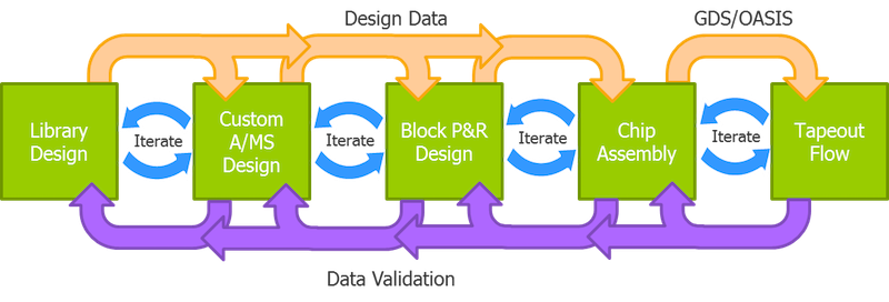
Figure 1: Data validation checkpoints at each design phase ensure bad data is not referenced in subsequent implementation phases and tapeout (Mentor)
There are three critical data validation tasks in a design flow:
- Ensure the most current P&R LEF data matches the chip-level GDS or OASIS data.
- Confirm the most current IP GDS/OASIS cells are in the final design before tapeout.
- Ensure that front-end-of-line (FEOL) data remains unchanged in staged tapeout flows (e.g., FEOL data is taped out before back-end-of-line (BEOL) data).
Typical data comparison techniques can require lengthy runtimes. Some design verification tool suites provide utilities that can be used in data validation flows to both shorten XOR runtime on large input designs and to validate data integrity beyond a simple layer comparison. If you are not already using these utilities, you are missing out on an opportunity to improve data integrity while reducing your time-to-tapeout.
LEF data validation
In a parallel design implementation flow, a sub-block design footprint (including pin locations and blockages) is used to define constraints for the block designers, and is converted to LEF for use as a P&R abstract for block instances in the chip-level design. The footprint and constraints defined by the block or chip-level floorplan provide a common starting place for both the block and chip-level designers, but may change as the design progresses. A failure to communicate floorplan changes to the block designer may result in errors later in the design process, when the GDS or OASIS block is merged with the chip-level design.
Similarly, requests from block designers to change the footprint and other requirements at the chip level may be agreed to by both groups, but run a similar risk of error if the updated block-level LEF data is not shared with the chip-level design team. Ensuring that both the block- and chip-level design teams have the most current and matching data can prevent delays that result from out-of-sync abstracts.
Traditional XOR comparison flows do not directly read LEF data, but LEF data can be converted and mapped to GDS or OASIS, typically using utilities provided in your design verification tool suite. Objects in the LEF data should always be mapped to their corresponding shapes in the block GDS. By their very nature, LEF representations are ‘abstract’, and may not contain the same objects as in a GDS or OASIS representation of the same block.
Fortunately, the block boundary and pin locations are expected to be the same, and serve as good correspondence points for comparison. For example, if the block GDS is exported such that M3 pins are on layer 3, datatype 0, and the boundary is output on layer 100, datatype 0, a LEF mapping file can be specified to match the output layers. You can then compare the converted data using traditional XOR tools. Any changes to the block footprint, or pin shapes that have moved, will be detected.
However, this validation method still cannot account for pins that have been swapped. For example, if the block contains M3 pins A and B, simply converting these shapes from LEF to GDS as shown in these commands does not distinguish between the pins. If pin locations remain the same, but the pin names change, this simple XOR comparison cannot identify the swap (Figure 2). A similar issue can occur with LEF obstruction (blockage) objects. Changes to blockage properties like SPACING cannot be detected by geometric XOR checks.
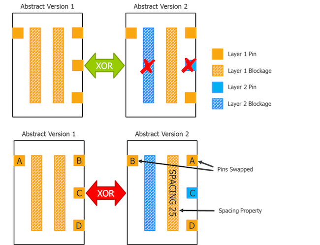
Figure 2. XOR can identify layer changes between LEF abstracts, but pin swapping or property changes to blockage objects are missed, and result in out-of-sync P&R abstracts (Mentor).
One way to address this issue is to map pin names and blockage spacing values to properties in the output GDS or OASIS file attached to the respective pin or blockage shape. The databases can then be compared using a process that compares objects and their properties, and reports any topological differences. Using this flow captures any true differences between the LEF pins and GDS pins that cannot be identified by XOR alone.
IP tapeout data validation
One important validation step often overlooked at tapeout is to confirm that any hard IP or other blocks that have been through multiple design iterations are current. Data exported from P&R may inadvertently merge outdated IP references into the output database. These blocks may pass layout vs. schematic (LVS) and design rule checking (DRC) verification, yet still not include some intrinsic changes required for manufacturability or optimum performance. Failure to verify the correct versions of IP are included in the final design database could impact yield or reliability down the road.
You should always verify that the IP blocks placed in the final chip design represent the latest version of these blocks. However, because there is no single version of the design that is guaranteed to have all the latest IP blocks, there is no way to perform a direct compare of the entire design. What you really need is a comparison between the latest IP GDS/OASIS, and the cell defined in the final chip-level GDS database. To use XOR to verify that multiple IP blocks match between the IP reference database and the chip-level database, you would have to run a unique XOR job for each cell. Because the XOR runtime would include reading both databases, the runtime required for such a flow would be prohibitive.
An alternative to running multiple XOR jobs is to use the object/property comparison process discussed earlier to compare the IP reference library cells against the chip-level database in one execution (Figure 3). This process should be able to perform a cell-to-cell comparison of references, polygons, paths, and (optionally) text between matching cell names in each design. Using this flow, database read-time occurs only once per design, and can quickly identify whether or not like-named cells referenced in the current and reference databases are the same or different. Any differences must be investigated further before tapeout. Note that neither the top-level design and cells or blocks in the chip-level database, nor the cells and blocks in the input IP databases, will be compared.
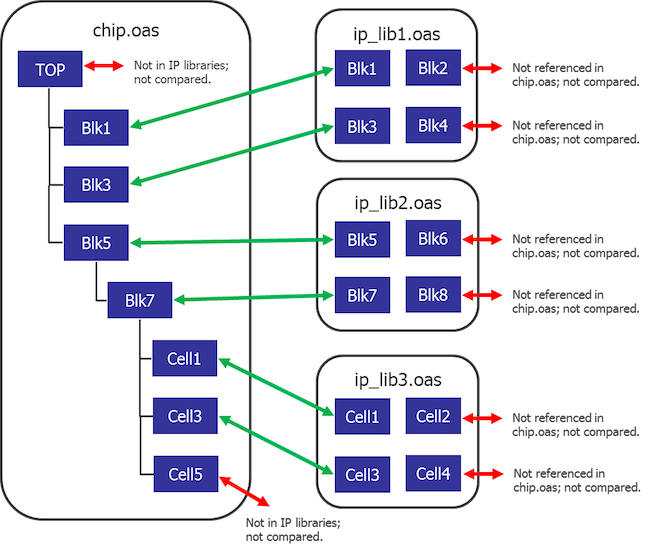
Figure 3. Compare the chip-level database against the latest versions of IP databases to validate the correct versions of cells and blocks are referenced in the design being taped out (Mentor)
Data validation for FEOL/BEOL tapeout
Taping out FEOL device-creation layers when no additional changes are expected allows the manufacturing process to start while the design team continues to work on BEOL routing and interconnect changes to meet timing closure and manufacturing requirements. At this point, the FEOL layers are essentially ‘frozen’, and no further changes should be made. Any intentional or accidental changes to a layer would likely require a costly new mask and lost time due to restarting manufacturing.
To ensure FEOL integrity, designers run LVL/XOR checks on the baseline design with frozen FEOL layers against their latest iteration with BEOL changes. While differences would be expected for the BEOL changes, any difference in FEOL layers is a red flag and must be investigated before proceeding.
Performing a full XOR compare is a reasonable final tapeout step, but there are better alternatives during design iterations. Running a full-chip XOR can be costly, since all the data on all the layers is processed. Runtime on dozens of CPUs could be many hours, and this process is often run overnight. As demonstrated with the IP checking flow, an object/property comparison utility can perform fast cell-versus-cell comparison, so combining such a utility with a DRC engine creates a process that can read input design databases and perform a cell-by-cell comparison to filter out cells from both input designs that 1) have not changed, and 2) have no interaction with objects that have changed.
The resulting subset of both input databases (containing the cells that have changed, and the data that interacts with objects in these cells) can then be sent to an XOR engine for further processing.
Conclusion
Maintaining design data integrity throughout a project with appropriate data comparisons can avoid some common pitfalls that often derail a project and impact tapeout schedules. A comprehensive data validation flow must ensure consistent data integrity for hard IP at tapeout, soft IP during design implementation, and staged FEOL/BEOL tapeout flows. Using data management utilities in conjunction with your DRC process can help fill the gap where traditional flows are lacking, while ensuring both fast and accurate data validation.
About the author
James Paris is a Technical Marketing Engineer with the Design to Silicon Division of Mentor, a Siemens Business, supporting Calibre design interfaces. Prior to joining Mentor, he was responsible for analog/mixed-signal physical design implementation and flow development for various IC design companies. James holds a B.S. in Computer-Aided Design Engineering and an M.B.A in Marketing.
