The fundamental question
Nanotechnology’s economic potential will only be harnessed through more basic research, according to a new report from the NSF. Paul Dempsey reports.
This year marks the 10th anniversary of the National Nanotechnology Initiative (NNI), and it is about a decade since the global sector analysis, Nano1, which led to its foundation. A good time to take stock not just of what has been achieved but also of what still needs to be explored, built and commercialized between now and 2020. Under the National Science Foundation (NSF) and the World Technology Evaluation Center (WTEC), the results of such an update, Nano2, are due for publication soon. According to one of the leading lights in the field, the verdict appears to stand somewhere between ‘promising’ and ‘could do better’.
Dr. Mihail Roco is formally the senior advisor to the NSF for nanotechnology and the founding chair of the National Science and Technology Council’s subcommittee on Nanoscale Science, Engineering and Technology. Informally, he is very much seen as the father of the NNI, the man whose brains and advocacy have helped sustain its $1b plus in annual founding, despite more recent federal cuts. Yet today, he thinks for all that investment, much of the challenge still comes down to basics—it is a view that will chime loudly with those of us who now see materials science as one of the most critical issues in securing the ‘more than Moore’ era for semiconductors.
At an NSF-hosted pre-publication hearing on Nano2, Roco said, “There are many things that are still open—even self-assembly. Self-assembly was so promising in 2000, but the first test measurements to see where atoms go and why they go there were done only a year ago—and we need that knowledge to understand fully what we can do.
“And we found that the situation [regarding fundamental research] is very similar throughout the world,” he said. “We found that sometimes a country’s focus was just to take an existing discovery and make a product in five years. That’s not bad in itself, but we need the balance where there is some contribution to continuing to develop the fundamentals.”
The numbers for nano-incorporated products released to market over the last decade support Roco’s position. Just six base materials are used in more than 90% of them, the foremost quartet of these being carbon nanotubes and nanoparticles formed of titanium dioxide, zinc oxide and silver.
Understanding these materials in more depth and, more importantly, adding more to the mix means that products could, in Roco’s view, create a global market worth $1t by 2015 and $3t by 2020 across all industries from approximately $300b today. And electronics stands to be to the fore of both making that growth happen as well as reaping its rewards. Beyond that, if the US really does face what President Obama has called a “Sputnik moment,” nanotechnology research must play a critical role in delivering the economic muscle that will maintain growth in GDP relative to the emergence of other global powers.
State of play
Nanotechnology is becoming a big business, with a lot of help from the public sector (Figure 1). In 2008, the EU led government funding at $1.7b, followed by the US at $1.6b and Japan at $950m. Others are ramping up public spending fast, with the same year seeing China pour in $430m, Korea $310m and Taiwan $110m. Korea also now leads Germany in terms of the sector’s Science Citation Index rankings, whereas in 2000, the country had no citations whatsoever.
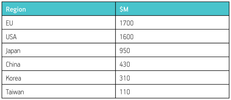
Figure 1
In the US between 2000 and 2008, related employment grew from 25,000 to 150,000 people, R&D spending from $370m to $3.7b, venture capital investment from $170m to $1.2b and product sales from $13b to $80b. An important subtext to those numbers is that private sector investment now exceeds that coming from the NNI and other US federal agencies. Growth for all these metrics stands between 25% and 35%, despite the recession.
However, the products coming to market point to a relative immaturity in our use of nanotechnology. According to Roco, we are currently working through two types of design. ‘Passive nanostructures’ are things like coatings that give us stain-resistant clothing and super-bouncy tennis balls. ‘Active nanostructures’ help us create more sophisticated items such as 3D transistors, targeted pharmaceuticals and adaptive structures.
The real game changers come in the next two categories: ‘Nanosytems’ leading to ‘Molecular nanosystems’. In these areas, we would be looking to progress from guided high-level assembly to bespoking molecules, from advanced but discrete-by-discipline hierarchical architecutures to those crossing multiple disciplines.
Moreover, much as in electronics, the world needs to undergo a shift toward system thinking where the applications comes first. This is why Roco believes that we still need broader fundamental research and he amplifies that argument by pointing out that we also need the tools to do that job.
“We are still in a formative phase, he said. “We are at the micro level—a shape and size approach, not an internal one [to understanding materials]. Only last year, did we start to see early measurements, a direct approach. Also, in manufacturing, almost all the processes we use are empirical. They are based on previous or existing technologies.”
Measure for measure
Roco identifies 12 target areas (see box, p.11) for the next decade of nanotechnology, including many familiar political, societal and economic ones. But he places metrology and simulation at the top of the list. The view is unanimous across the dozen other contributors to Nano2.
“Our periodic table is a bit daft,” says Dr. Chad Mirkin, one of the those other rapporteurs and director of the International Institute for Nanotechnology at Northwestern University. “We’ve defined things by size, shape and composition.”
Mirkin’s view is that as nanotechnology pushes science beyond spherical particles into such areas as rods, wires, prisms and platonic solids, we need a periodic table that works in multiple dimensions. Thermal, photochemical and electrochemical behavior—which can shift at the sub-atomic scale—also need to be considered.
He sees this as part of a critical interplay between three ‘pillars’ of nanotechnology: a fundamental pillar (of which a new periodic table would be a part along with other basic discoveries); an evolutionary/integrative pillar (using fundamental discoveries to enhance existing materials and processes, such as titanium
dioxide suncreen and semiconductor manufacturing); and a revolutionary pillar (taking lateral ideas from the fundamental domain to develop disruptive technologies).
As logical as all of this sounds, it represents a technological challenge that remains very fresh. That said, electronics is already playing a critical role in addressing it—partly because it is a field that has potentially a great deal to gain from closer materials understanding and characterization. The ‘Post-Silicon Era’ and all that.
One example of the advances being made was cited by another Nano2 contributor, Dawn Bonnell, director of the Center of Science and Engineering of Nanoscale Systems at the University of Pennsylvania. “Aberration correction is revolutionizing structural imaging in electron microscopy,” she said. “It allows atomic-level vision of atoms as light as oxygen.”
The Transmission Electron Aberration Correction Microscope project (see box) demonstrated equipment capable of resolution of 0.05nm in 2009. It is now being used to explore materials such as graphene, germanium and gold that are all expected to have a major impact on emerging nanotechnology applications. Similarly, Bonnell cited recent advances in synchroton radiation technology that have allowed observation of attosecond snapshots of electronic disturbances in water produced by diffusing gold ions. That implies rates of improvements in available brightness ahead of those being achieved in microelectronics under Moore’s Law.
It is a good start, but more is required. Looking toward 2020, Bonnell identified five leading targets, all of which, like the metrology advances above, would appear to require some major input from electronics alongside other disciplines.
- Atomic resolution of the 3D structure of a single protein with chemical specificity.
- Mapping the continuum properties of individual atoms in a solid and bridging the continuum and quantum regimes.
- Discovery of stable new compounds by the manipulation of atoms at room temperature.
- Tracking electrons with sufficient speed to observe intermediate steps in chemical reactions.
- Concurrent imaging of processes throughout an entire cell.
The poster child
Electronics has taken more steps into the world of nanotechnology than any other industry—without them contemporary scaling and performances boosts would have been impossible, never mind the work already under way to go to process nodes below 20nm.
Similarly, it is going to be one of the sector’s great enablers. Its importance to metrology is already demonstrable. Another Nano2 participant, Dr. James Munday of the University of South Carolina, added that it also offers opportunities for reuse. “One way to exploit the work of the semiconductor industry is that they leave behind many technologies that have been amortized but which can be coupled now into areas such as healthcare,” he said.
Some of this is already visible in micro-electromechanical systems (MEMS). Many older fabs—typically those running six-inch wafers—are being switched to foundry use for MEMS products in not just healthcare but a host of other industries. But in electronics-specific terms, Dr. Jeffrey Welser, director of the Nanoelectronics Research Initiative on assignment from IBM, offered an intriguing view. For example, as lithography for chip fabrication hits roadblock after roadblock, he suggested that that traditional top-down approach could be used down to 10nm but then combined with bottom-up self-assembly to reach 1nm. Manufacturing could also benefit from R&D into the near-atomic level control of materials in three dimensions.
However, his main theme was that—again—a ‘systems-based’ shift in thinking is required if the sector is to exploit much hyped materials and concepts like spintronics and magnetic tunneling. “We need,” he said, “increased focus on utilizing new nanoscale physics for device functionality rather than just fighting those physics to continue current device scaling.”
Architectures will change, carbon will play a greater role and the applications driving that system thinking will increasingly move beyond the traditional world of information technology into sensors, energy, medicine and more complex mobile devices. All that then will be enabled by more multi-disciplinary design practices. “Microelectronics was the economic driver of the last half of the 20th Century; nanoelectronics is poised to drive the first half of the 21st,” Welser said.
