System level DFM at 22nm
The article provides an overview of one common theme in the papers presented at a special session of the 2009 Design Automation Conference, Dawn of the 22nm Design Era. As such, we would recommend that readers wishing to access still more detail on this topic (in particular, on device structures for 22nm and project management requirements) read the original contributions in full.
The papers are:
- 8.1 “Design Perspectives on 22nm CMOS and Beyond”, Shekhar Borkar, Intel.
- 8.2 “Creating an Affordable 22nm Node Using Design-Lithography Co-Optimization”, Andrzej Storjwas, Tejas Jhaveri, Vyacheslav Rovner & Lawrence Pileggi, Carnegie Mellon University/PDF Solutions.
- 8.3 “Device/Circuit Interactions at 22nm Technology Node”, Kaushik Roy, Jaydeep P. Kulkarni, Sumeet Kumar Gupta, Purdue University.
- 8.4 “Beyond Innovation: Dealing with the Risks and Complexity of Processor Design in 22nm”, Carl Anderson, IBM.
 The 2009 Design Automation Conference was held in San Francisco, July 26-31, 2009. Further information on accessing archived proceedings and papers presented at the event is available at www.dac.com.
Special Digest, EDA Tech Forum
A recent session at the Design Automation Conference in San Francisco considered how to make the 22nm process node a reality despite an increasing number of obstacles. All the speakers were unanimous that part of the answer will come from using system-level design strategies to address manufacturability.
Much has already been said and written about the need to bring design-for-manufacture (DFM) further up the design flow, although it would appear that necessity will prove as much the mother of abstraction as invention in this case, with 22nm creating a series of challenges that make the shift necessary.
According to various data, 22nm manufacturing is expected in 2012 and leading manufacturers are already installing or preparing to install capacity (Figure 1).
Source: Intel
|
High Volume Manufacturing |
2006 |
2008 |
2010 |
2012 |
2014 |
2016 |
2018 |
|
Technology Node (nm) |
65 |
45 |
32 |
22 |
16 |
11 |
8 |
|
Integration Capacity (BT) |
4 |
8 |
16 |
32 |
64 |
128 |
256 |
|
Delay = CV/I scaling |
~0.7 |
>0.7 |
Delay scaling will slow down |
||||
|
Energy/Logic Op scaling |
>0.5 |
>0.5 |
Energy scaling will slow down |
||||
|
Variability |
Medium |
High |
Very High |
||||
FIGURE 1 Technology outlook
The challenges of 22nm
Intel
Intel has always been at the forefront of the intersection between design and manufacturing, and remains one of the few semiconductor companies fully active in (and committed to) both areas.
Shekhar Borkar, a company fellow and director of its Microprocessor Technology Labs, divided the challenges presented by the 22nm into the technological and the economic, and also made some observations on the future of custom design. His overarching theme was that ‘business as usual’ simply is not an option.
From the technological point of view he cited a number of relatively familiar but now increasingl large problems. The main ones were:
- slowdowns in gate delay scaling;
- slowdowns in both supply and threshold voltages as subthreshold leakage becomes excessive;
- increased static variations due to random dopant fluctuations (RDFs) and the limitations of sub-wavelength lithography (stuck at 193nm, with ‘next-generation’ extreme ultra-violet (EUV) lithography still to arrive in commercial form);
- increased design rule complexity and more restrictions due, again, largely to sub-wavelength lithography; and
- greater degradation and less reliability due to the high electric fields.
- From the economic point of view, Borkar noted that:
- Intel expects a 22nm mask set to cost more than $1M, indicating that the manufacturing cost ramp is hardly slowing down (separately, the Globalfoundries fab being prepped for 22nm has been ‘conservatively’ estimated at a cost of $4.5B); and
- there is a growing ‘tools gap’ between increases in efficiency that are being delivered and the ability of the EDA software to deal with the increases in complexity presented by a node that is likely to offer one billion transistors on a single piece of silicon.
- Then, Borkar described how the traditional advantages of custom design would be reduced or obviated completely:
- Achieving the best operational frequency is no longer achieved largely by optimizing the resistance and capacitance metrics for interconnect, since transistor scaling, variability and power consumption have increased their influence so greatly.
- The restricted design rules (RDRs) imposed by manufacturing variability virtually eliminate the chances of going in to manually enhance how closely transistors and interconnects are packed together on a chip.
- There have been cases where attempts to take a local rather than a global view of optimization, in the hope that there may be some islands available, have actually worsened rather than improved a design, or at least added to the time-to-market to little effect.
Carnegie Mellon/PDF Solutions
In his presentation, Andrzej Strojwas, Keithley professor of Electrical and Computer Engineering at Carnegie Mellon University and chief technologist of PDF Solutions, echoed many of Borkar’s points and added some observations of his own, more directly related to manufacturing metrics.
It is his belief —and that of his CM/PDF co-authors—that the recent, highly lauded innovations in high-k metal-gate stacks will reduce RDF-based variation only for the 32/28nm process generation. For 22/20nm, the industry will need to move to long-touted device architectures such as FinFETs and ultra-thin-body or fully depleted silicon on insulator (SOI), technologies that mitigate RDFs by reducing the dopant concentration in the channel.
Furthermore, CM/PDF research suggests that systemic variations will reach prohibitive levels at 22nm if issues surrounding limitations in lithography resolution and the design enhancements offered through stress technologies are not addressed. In particular, the ongoing lack of EUV lithography is forcing the introduction of double patterning techniques (DPTs). In context of the modeling, characterization and printability challenges such multi-exposure DPTs suggest, the technique will be extremely expensive.
Purdue University
Kaushik Roy, professor in the Nanoelectronics Research Laboratory at Purdue University, joined Strojwas in putting forward a structural answer to the challenges presented by 22nm.
In Purdue’s case, one proposal was for multi-gate FETs (MUGFETS) to address the increase in short channel effects (SCEs) as shrinking transistor sizes bring the source close to the drain.
Source: Purdue University
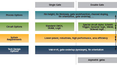
FIGURE 2 Technology-device-circuit-system codesign options for double gate MOSFETS from 22nm
MUGFETS will not be immune to SCEs—nor to threats from body thickness—but they do offer a broader range of design elements that can be tuned for the node. These include multi-fin and width quantization, use of the back-gate as an independent gate, gate-underlapping and fin orientation (Figure 2). An important question, though, is where in the flow such tuning should take place.
IBM
Carl Anderson, an IBM Fellow who manages physical design and tools for the company’s server division, addressed the challenges inherent in 22nm from a project management perspective.
As complexity increases, he argued, so does the emphasis that needs to be placed on the culture and discipline through which companies manage risks and resources.
Even today, respins and major delays could often be attributed to changes that were sought relatively late in the design cycle, he said.
He also warned that “It will be very easy and tempting to propose chip designs and goals for 22nm that are unachievable within finite schedules and resources.”
The system-level solution
Given the variation in topics across the four presentations, there was nevertheless broad agreement that some kind of high-level design flow strategy needs to be adopted to take full account of 22nm’s sheer range.
Correct-by-construction
The notion of abstracting to the system level to achieve correct-by-construction design was cited explicitly by both Borkar and Strojwas. Borkar said the main objective had to be designs that are fully functional, on specification and manufacturable after the first past. To do this, he said that the industry needs to shift to a system design methodology that is “SoC-like” [system-on-chip].
Source: Intel
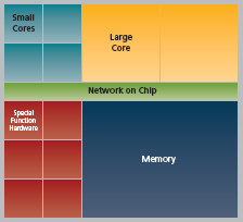
FIGURE 3 SoC-like design methodology with ‘soft’ macros
The main difference will lie in the fact that today such SoC strategies are based around application-specific blocks, whereas that required for 22nm will be more concerned with soft blocks (or macros) that represent such components of a design as cores, on-die networks and some ‘special function’ hardware (Figure 3). At the same time, Borkar said that the shift to place more of the overall system onus on software will continue.
These new blocks will be predesigned and well characterized, and as a result, the emphasis in differentiating your product and enhancing its performance will move to system-level optimization as opposed to designing logic blocks. Physical design will also be predominantly automated, and numerous aspects of a design might now be ‘hidden’ from the designer (e.g., clocking).
There would be still more integration required to meet the needs of the test stage, Borkar said, with each functional block requiring either built-in self-test capability or a straightforward interface to an external tester.
Strojwas defined goals that addressed a traditional set of DFM objectives more specifically, but also placed great emphasis on pre-characterized circuit elements and templates. This may suggest a slightly greater degree of granularity than Borkar’s vision, although to say as much to any major degree would be splitting hairs.
Strategically, Strojwas says that DFM must become proactive as opposed to reactive, notwithstanding its inherent need to operate based on a considerable volume of already generated and deeply researched manufacturing data (indeed, exactly the kind of analysis in which PDF Solutions specializes). This alone will effectively counter systemic variation, he said.
Source: Carnegie Mellon University/PDF Solutions
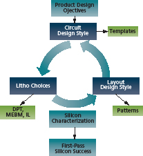
FIGURE 4 Extremely regular layout methodology
In the paper that accompanies the DAC presentation, Strojwas and his co authors write, “We propose a novel design methodology (Figure 4)…that will ensure a correct-by-construction integrated circuit design.” They continue:
The key enabler of the methodology is the creation of a regular design fabric onto which one can efficiently map the selected logic templates using a limited number of printability friendly layout patterns. The co-optimization of circuit layout and process is achieved by selection of logic functions, circuit styles, layout patterns and lithography solutions that jointly result in the lowest cost per good die. The resulting set of layout patterns and physical templates are then fully characterized on silicon through the use of specially designed test structures.
Roy and Anderson are looking at this from less specifically methodological aspects, but where their papers intersect, they reach broadly similar conclusions.
Roy and his co-authors conclude their review of various device structures by noting that system-level strategies are already developing that are independent of the underlying technology, and continue by stating:
Technology scaling in 22nm [will] require closer interaction between process, device, circuit and architecture. Co-optimization methodologies across different levels [will] help to mitigate the challenges arising due to changes in transistor topology and increased process variations. Novel device/circuit/system solutions integrated seamlessly with the EDA tools [will] help meet the desired yield and [will] help the semiconductor industry to reap the benefits of scaling economics in sub-22nm nodes.
With his focus on integrating tools and design methodologies into project management—arguably one of the more neglected areas in terms of EDA implementations and executions—Anderson notes that design teams will need to make still more numerous and complex trade-offs between schedule, function, performance, cost and resources for 22nm. He continues:
Trade-offs between custom vs. synthesized macros, reused vs. new custom [intellectual property], more features vs. power, etc. will have to be made early in the design cycle. The challenge will be to optimize the entire chip and not just a single component.
However, given the threats posed by late-stage changes or “problems that are hidden or that only surface near the end of the design cycle,” and the fact that the ability to address them may be constrained, he also notes that a good engineer’s ability will continue to be defined by whether or not he can innovate “inside the box.”
Cultural change
Until very recently, DFM and ESL have been seen as two very different areas of endeavor within EDA and chip design more generally. There has also been a perceived geographic split, with North America being considered stronger on manufacturability issues while Asia and Europe were considered more advanced in terms of abstracted design flows.
The message from manufacturing specialists at 22nm, however, is that its distinction is becoming increasingly untenable. The minutiae of a circuit or a transistor still matter—indeed, the structure of circuits would seem fundamental to any progress along the process node path—but systems that are defined with an awareness of fabrication challenges are vital to future progress.
