STIX to the task
Before 2001’s historic downturn, the semiconductor industry was primarily driven by the corporate and enterprise markets. This bias led to a somewhat predictable three-year business cycle of peaks and troughs. Corporate buying practices, technology requirements and IT replacement policies are all relatively easy to predict—right down to the nature of the semiconductors that underpin the main end products.
Since 2001, however, consumer electronics has formalized and built upon its position as the primary market for ICs. This has created a much more volatile business environment.
Not only are there many different consumer electronics offerings (and therefore many different ICs), but also the success or failure of any end product is hard to predict. Even the prevailing macroeconomic trend—be it up or down—will often offer little clue of how a certain item will fare.
Given such volatility, today’s semiconductor companies must be able to design products quickly and ramp up production steeply even in the light of uncertain volume forecasts—‘killer’ applications often give few clues beforehand of the demand they will achieve. Meanwhile, consumers themselves demand, and usually get, rapid price reductions once a product approaches mass-market penetration. This cost-down requirement places further stress upon the supply chain, because it often runs ahead of the economies the industry achieves by implication from Moore’s Law.
Overall, the continuing shift toward a more high-risk operating environment places a premium on identifying and implementing cost and operational efficiencies throughout the supply chain, with obvious implications for the silicon design flow. Therefore, the value of those efficiencies that can be gained through standardization is greater than ever. Semiconductor test is no exception in this regard—indeed, given other technological trends, it is arguably a priority.
The demands of the consumer market are also driving up the complexity of today’s ICs. Typical system-on-chip (SoC) designs integrate a wide variety and number of technologies including microprocessors, memory, digital, analog, mixed-signal and RF. It is hard enough to test such highly integrated devices to an appropriate fault coverage and quality level under ‘traditional’ development criteria; to be able to do so for those set by the consumer electronics space is especially daunting and demands creative solutions.
Design for manufacturing (DFM) has greatly increased in importance at deep-sub micron process geometries. As a result, a huge range of design tools, wafer fab, and packaging & test technologies has emerged to support the new DFM philosophy. This trend has exposed the fact that decisions once left to the ‘back-end’—such as the choice of test methodology and final die format (known good die, packaged die, SIP, etc.)—must today be considered toward the front of the design flow so that they properly reflect today’s technological and time-to market requirements.
The overall result is that the supply chain has become compressed, as has the shelf life of the resulting ICs. We need to undertake a fundamental and broad-based review of how we produce leading-edge products.
More with less
Would it have made sense for the PC industry to have had two or more variants of the Universal Serial Bus (USB)? Not really. By ultimately adopting this open standard, the industry enjoyed all the benefits associated with economies of scale by enabling suppliers to focus their R&D efforts on producing innovative devices, without giving up any critical intellectual property (IP). So, can we apply similar thinking to the challenge posed by test in the realm of chip design today? Yes, we probably can. Although you would not say that interfacing a state-of-the-art tester with an equally advanced wafer prober or handler is of exactly the same complexity as what is achieved on PCs with USB, the same basic principles apply and, therefore, the same type of benefits can be achieved.
Standardizing automated test equipment (ATE) interfaces through non-proprietary IP is now essential to the development of the entire semiconductor supply chain. It enables companies to efficiently run production volumes by leveraging economies of scale—indeed such economies will also be available for more modest production runs.
It provides an ability to quickly move manufacturing solutions around the test floor—critical to maintaining high utilization rates on expensive equipment and thus directly driving cost efficiencies for integrated device manufacturers (IDMs) and outsourced semiconductor assembly and test (OSAT) service providers.
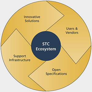
Figure 1. The STC Ecosystem aims to promote an open, collaborative environment. Source: STC
Finally, equipment suppliers will benefit from no longer needing to develop proprietary interface IP that does not actually differentiate the quality of the end products. STC These business challenges and objectives caused a group of leading semiconductor players—led by Advantest, Intel and Motorola SPS (now Freescale Semiconductors)—to set up the Semiconductor Test Consortium in 2003, with the overall objective of delivering a synergistic, industry-wide ecosystem for test. The four key elements of the STC Ecosystem (Figure 1) are:
- Users and vendors working collaboratively.
- Truly open specifications that everyone in the supply chain can access.
- A support infrastructure that facilitates the solutions development process.
- Highly innovative test solutions for rapid deployment.
The Consortium’s initial efforts focused on the ATE and the Open Semiconductor Test Architecture hardware and software specification, better known and today increasingly widely adopted as OPENSTAR. Based on evolving member and industry demands, STC launched the Semiconductor Test Interface eXtensions (STIX) initiative in 2007, and this specifically extended the consortium’s remit to standardizing the interfaces around ATE, which are treated as non-architecture-specific ‘black boxes,’ regardless of vendor.
In many instances, ATE capital costs represent only 25-30% of the total cost of test. The mostly untapped balance of cost savings can be found in the many areas around the core hardware. These include hardware docking, data and program portability and software tools (Figure 2), which are perfect candidates for some level of standardization.
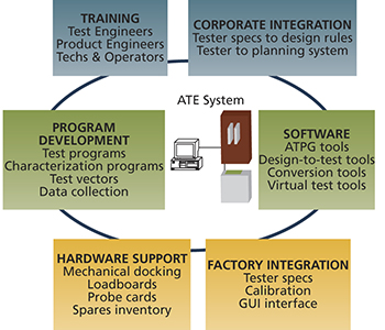
Figure 2. Critical cost reduction areas around ATE. Source: STC
Working through STIX
To fully realize some tangible value from open, pre-competitive collaboration, the STC has formed several STIX working groups (Figure 3).
The Probe Card Working Group (PCWG) was set up by members in Japan. They are addressing the important task of accurately coordinating user and vendor information across multiple manufacturing sites. The three areas they have initially addressed are the probe card order placement flow, the mechanical holder and the specification order sheet. By standardizing this trio, they expect to minimize costs, reduce communications errors and cut the time it takes to get probe cards into production.
The Docking and Interface Working Group (DIWG) was formed in early 2007. Its work is driven primarily by European STC members and covers such a diverse range of areas that its main activities are now split across five sub-groups (docking & interfacing, handler, manipulator, prober and tester).
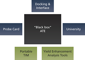
Figure 3. STIX Working Groups. Source: STC
The University Working Group (UWG) is made up of 40 academics from institutions throughout the world. There is grave anxiety that the global education system is not keeping up with the demands of the industry. There are also concerns that college graduates often require six to 18 months of further training in test engineering before they can be considered fully productive. The UWG’s main objectives are to drive closer alignment between industry and academia, promote university research (starting with the establishment of a global database of research projects), provide a repository for test engineering curriculum information, and partner with other industry organizations.
The Yield Enhancement Analysis Tools Group (YEATG) addresses how to handle the vast array of test data that is now necessary to efficiently run high production volumes, especially when managing multiple offshore locations and working with OSATs. This task is increasing in importance as the fabless model becomes so well established that even major IDMs now outsource much (in some cases, almost all) of their manufacturing.
The Portable Test Instrument Module Group (PTIMG) is being set up to define hardware and software interface standards that will enable users to quickly and cost-efficiently incorporate ancillary test instrument solutions into the ATE environment. This is especially critical to meeting the dynamic and often unpredictable consumer market in a timely manner.
Participation in these and other STC activities is open to all companies that are involved in any aspect of semiconductor test. Their latest findings will also be discussed at the forthcoming Global STC Conference in San Diego (June 4-6, more information at www.semitest.org/events/GSC_2008)—and although STIX is a relatively new initiative, much has already been achieved. Appropriately, this year’s conference theme is “Collaborative Solutions Beyond 2010,” and the event has partnered with both the Design Automation Conference (DAC) and the Semiconductor Wafer Test Workshop, affirming the degree to which holistic solutions are required for the challenges the industry faces.
Towards tomorrow
The technological and business needs for new ATE interface standards that benefit the entire supply chain have never been more visible. The days of throwing a design over the fence and having a test engineer successfully deal with it are long gone. The technological complexities of today’s SoC devices and associated assembly and packaging stages require a concurrent engineering approach that comprehends test methodologies prior to the design phase. At the same time, consumers expect all aspects of an end product to have been tested to a very high quality, but at minimal cost.
Given these boundary conditions, the semiconductor supply chain must be able to fully leverage the vast technological and economic advantages of standardized test interfaces, to enable innovative solutions, create economies of scale and shorten time-to-market/volume/profit. The STC is contributing to this overarching goal through its STIX initiative.
Keith Imai is the STC Manager for Advantest America, and chairs the STC Marketing Working Group.
