When good DFT goes bad: debugging broken scan chains
Scan chains help you test complex chip designs. But how do you test the scan chains themselves when they go wrong?
The advent of on-chip compression, built-in self-test (BIST), and fault models targeted at leading-edge process nodes have cemented the position of scan-based testing as the most powerful design-for-test (DFT) method for digital semiconductor devices. Since chain elements are based on the sequential elements of a design, they can easily occupy 30% of a chip’s area and can account for up to 50% of chip failures [1]. Since Murphy’s law still prevails, and everything that can go wrong eventually will go wrong, having the ability to effectively debug broken scan chains is therefore crucial for test pattern bring-up, failure analysis, and yield learning.
Detecting scan-chain defects
The most effective way to test the scan chains, and to detect any broken scan chains, is using a dedicated ‘chain test pattern’ or ‘chain flush’ pattern. A chain test simply shifts a sequence, typically ‘00110011’, through the entire scan chain without exercising the functional circuitry. The pattern that appears on the device output pins is expected to be exactly the same sequence that’s shifted in, assuming there are no inverters along the chain. Any defect in the scan chain will be observed by the tester on the scan output pins, as shown in Figure 1.
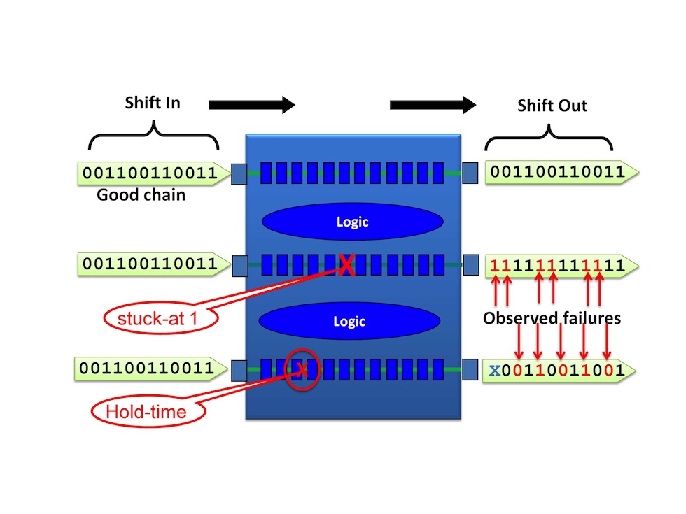
Figure 1
Using a scan chain test to observe failing scan chains (Source: Mentor Graphics – click image to enlarge)
The chain test results also help us understand the type of defect that haunts our scan chains. As shown in Figure 1 and for additional models in Table 1, different defect types will yield different chain test results. A single delay defect will, for instance, result in the correct sequence appearing at the output pins, but with a one-cycle offset.
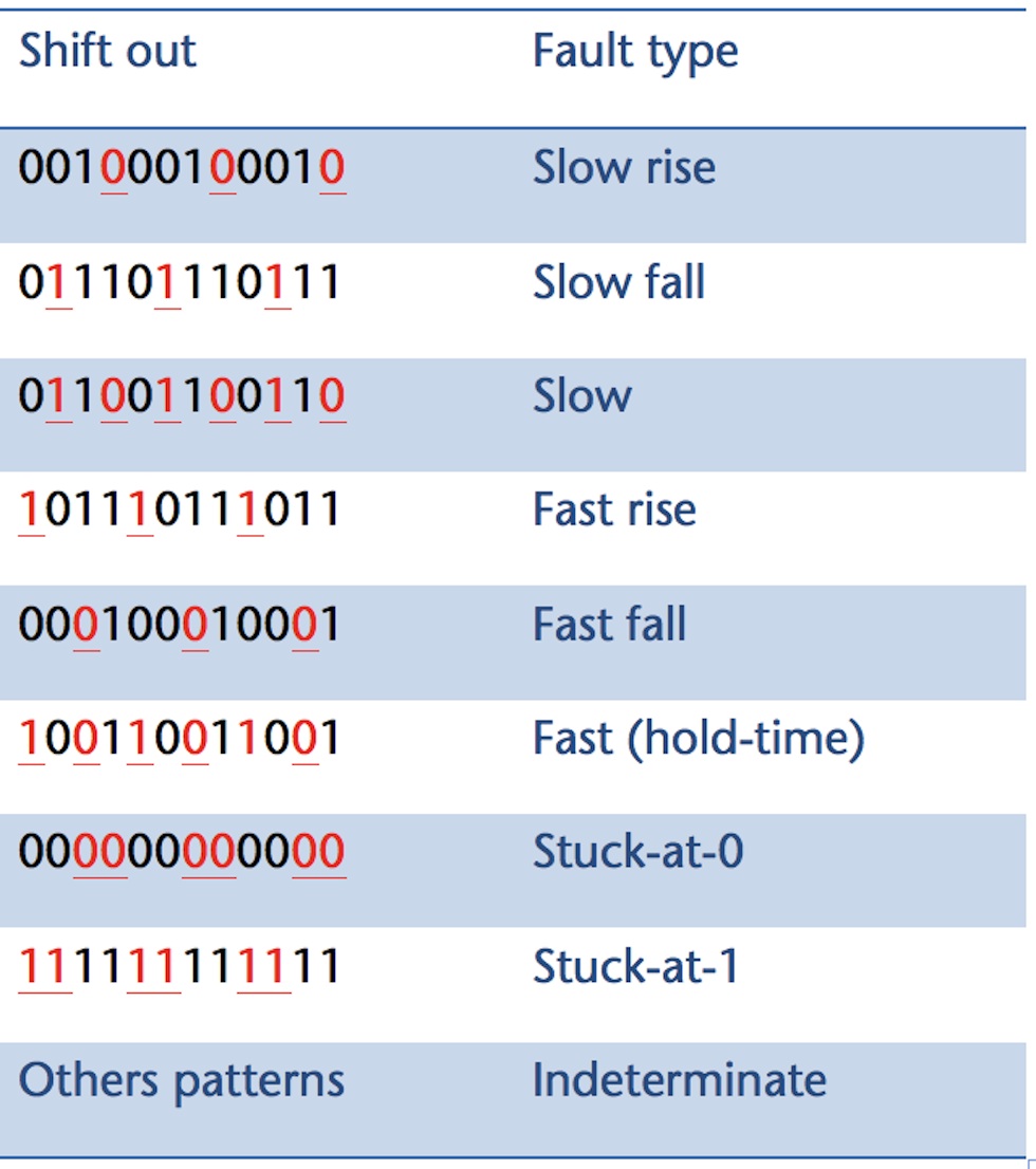
Table 1
Chain fault models determined by chain patterns (shift-in: 001100110011) (Source: Mentor Graphics – click image to enlarge)
Location, location, location
While detecting a scan chain defect is trivial, identifying the defect location is much more complex. Knowing the exact location of the defect is crucial for bring-up, failure analysis (FA), and debug applications. The chain test results will not give any indication of where in the chain the defect is located. Depending on the type of defect, it is also virtually impossible to determine how many defects exist on each failing chain.
Since we cannot identify the defect location from the chain test results, we have to take a more sophisticated approach. There are four general ways of identifying scan chain defects. These are:
- Tester based techniques such as on-tester fault targeted patterns [2]
- Physical failure analysis based techniques such as laser modulation mapping [3]
- Modified scan architectures [1]
- Software based diagnosis [1]
This article focuses on software-based diagnosis, which is based on production test results and does not require any additional test time or dedicated hardware equipment. Software-based diagnosis is offered by all commercial automatic test pattern generation (ATPG) tool vendors, and is loosely based on ATPG technology.
A typical flow for scan-chain diagnosis is shown in Figure 2. An ATPG software tool is initially used to generate test patterns for a device. These patterns include chain patterns and the scan patterns that target faults in the functional circuitry of the design.
When these patterns are executed on the tester (ATE), failures have to be collected for both the chain patterns and the scan patterns. Typically, failures from at least 32 scan patterns are required to achieve good diagnosis results. The diagnosis software then uses the gate-level representation of the design, test patterns, and the tester fail data to identify the location and type of scan-chain defects.
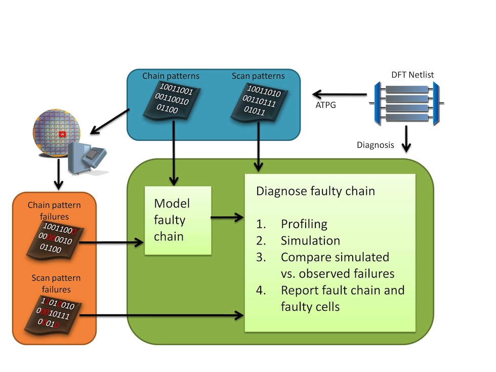
Figure 2
Scan-chain diagnosis flow (Source: Mentor Graphics – click image to enlarge)
A typical diagnosis tool will use a collection of algorithms to provide the best possible results, but to get a basic understanding, we will take a closer look at the simulation technique, shown in Figure 3.
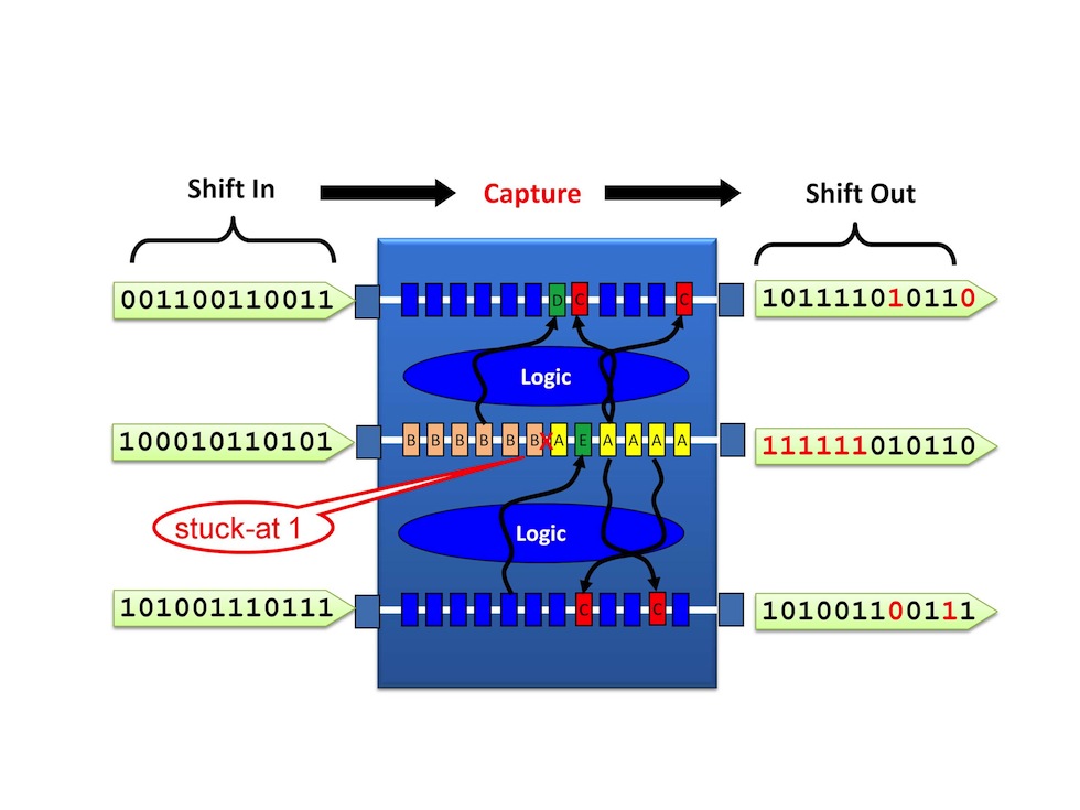
Figure 3
Simulation of scan patterns to identify failing cell location (Source: Mentor Graphics – click image to enlarge)
In this example, there is a ‘stuck-at’ defect in one of the scan chains. When a scan pattern is shifted into the chains, all the cells on the input side of the defect (labeled B in Figure 3) are correctly loaded, but the defect corrupts the cells on the output side of the defect, so that these cells may have incorrect values. During the scan capture, the loaded values propagate through the functional circuitry and may be captured in other scan cells. Cells with fan-ins, including the incorrectly loaded scan cells (labeled C), may capture incorrect values, while cells with inputs fanning in from the correctly loaded scan cells (labeled D), capture the correct data. When data is shifted out of the chains, the cells on the input side of the chain defect (B) will be corrupted so that incorrect values may occur on the output pins, while the cells on the right side of the defect that are fed by data from good chains (E) will capture correct data.
By now you may have noticed the use of the word “may” in the previous sentences. Whether or not incorrect data is captured as a result of the defect depends on whether the faulty behavior differs from the expected behavior. For instance, if the expected value for all the ‘B’ cells is 1, then no failures will be observed when the pattern is shifted out. By analyzing the failures from multiple failing scan patterns, and tracing failures back to the origin, diagnosis tools can use this simulation approach to identify the failing locations.
Taking scan-chain diagnosis to the next level
The simulation approach alone may be insufficient to provide accurate results, especially in cases of multiple and intermittent defects. For large designs, simulation runtimes can be very high due to the amount of fail data that has to be simulated. New techniques have therefore emerged to help address these concerns. Profiling [4] and dictionary-[5] based approaches can help improve accuracy, resolution, and runtime. Technology has also been developed to ensure that diagnosis is compatible with on-chip compression [6]. These new approaches make scan-chain diagnosis a viable solution for even the largest designs for both low-volume applications such as failure analysis, and volume diagnosis applications for yield analysis [7-8].
Case Study
In a recent study, a semiconductor company suffered from lower than expected yields on certain wafers of several products on a relatively new 40nm process [9]. More than 50% of die with failures in the digital circuitry were caused by scan-chain defects. To increase the chance of successful physical failure analysis (PFA) results, fail data was collected from about 100 failing die. Of these, 61 devices had diagnosis results deemed good enough to be used as starting point for PFA. The requirements were set to a diagnosis score larger than 95, a diagnosed chain segment of less than three scan cells, and less than four faulty scan chains. Five devices with the best diagnosis results were selected for PFA, and defects correctly identified in all five cases, as indicated in
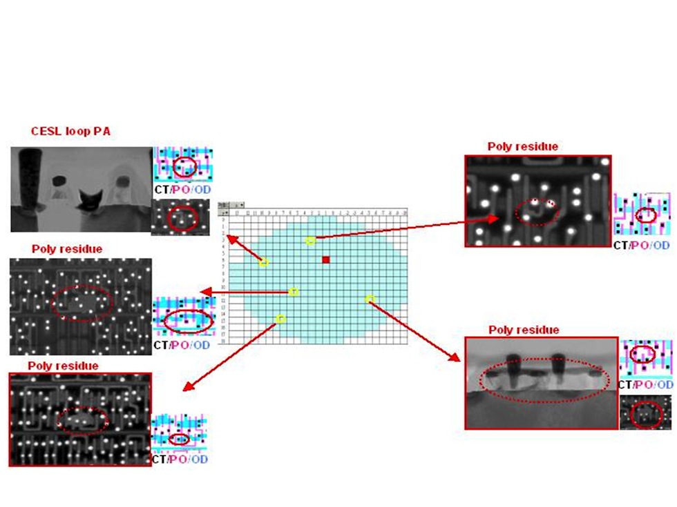
Figure 4
Physical failure analysis images from locations identified by scan chain diagnosis (Source: Mentor Graphics – click image to enlarge)
Of the five devices analyzed, poly residue was found in four. The last device had a defect at the closed-loop contact-etch stop layer (CESL).
Conclusion
Software-based scan-chain diagnosis is an effective and automatable tool for debugging broken scan chains as part of a device bring-up, failure analysis, and yield-analysis process. The technology has been proven by many industrial cases for a wide range of scenarios [10].
References
[1] Y. Huang, R. Guo, W.-T. Cheng, J. C.M. Li, “Survey of Scan Chain Diagnosis”, IEEE Design and Test of Computers, May 2008, pp. 240-248.
[2] A. Crouch, “Debugging and Diagnosing Scan Chains”, Electronic Device Failure Analysis, January 2005, pp. 16-24
[3] S. Kasapi, W. Lo, J. Liao, B. Cory, H. Marks, “Advanced Scan Chain Failure Analysis Using Laser Modulation Mapping and Continuous Wave Probing”, Proc. of International Symposium of Testing and Failure Analysis (ISTFA) 2011, pp. 12-17. www.asminternational.org.
[4] Y. Huang, W.-T. Cheng, R. Guo, T.-P. Tai, F.-M. Kuo, Y.-S. Chen, “Scan Chain Diagnosis by Adaptive Signal Profiling with Manufacturing ATPG Patterns”, Asian Test Symoposium (ATS) 2009, pp. 35-40.
[5] R. Guo, Y. Huang, W.-T. Cheng, “A complete test set to diagnose scan chain failures”, Asian Test Symoposium (ATS) 2007, pp. 1-10.
[6] Y. Huang, W.-T. Cheng, J. Rajski, “Compressed pattern diagnosis for scan chain failures”, IEEE International Test Conference (ITC) 2005, pp. 744-751.
[7] C. Schuermyer, B. Benware, G. Rhodes, D. Appello, V. Tancorre, O. Riewer, “Device Selection for Failure Analysis of Chain Fails Using Diagnosis Driven Yield Analysis”, Proc. of International Symposium of Testing and Failure Analysis (ISTFA) 2011, pp. 91-97. www.asminternational.org
[8] F.-M. Kuo, Y.-S. Chen, “Yield Ramp up by Scan Chain Diagnosis”, Asian Test Symposium (ATS) 2009, pp. 94-95.
[9] Y. Huang, B. Benware, W.-T. Cheng, T.-P. Tai, F.-M. Kuo, Y.-S. Chen, “Case Study of Scan Chain Diagnosis and PFA on a Low Yield Wafer”, IEEE International Test Conference (ITC) 2010, poster.
[10] Y. Huang, “Yield Improvement by Scan Chain Defects Diagnosis”, ASM International webinar, http://www.mentor.com/products/silicon-yield/multimedia
About the Authors
Geir Eide earned an MS in electrical and computer engineering from the University of California at Santa Barbara and is a product marketing manager in the Silicon Test Solutions group at Mentor Graphics Corporation. He can be contacted at geir_eide@mentor.com.
Yu Huang earned a PhD in electrical and computer engineering from the University of Iowa and is a software developer in the Silicon Test Solutions group at Mentor Graphics Corporation. He can be contacted at yu_huang@mentor.com.
