Silicon carrier for computer systems
Applications ranging from gaming to digital media to data analytics continue to grow more complex and constantly demand increasing computing power from computer systems. Historic growth in microprocessor performance has primarily been responsible for assuring a steady growth in the computing power of computer systems. Traditionally, this growing performance has been sustained by scaling down the minimum dimensions of CMOS devices and increasing the number of transistors on chip. In recent years, however, the difficulties encountered in scaling CMOS devices beyond 45nm and increasing power dissipation have substantially limited the historic growth of microprocessor performance. It is clear that unconventional methods that focus beyond scaling are needed.
At the system and packaging level, one such method involves the use of silicon carrier technology that can provide high I/O density, high speed signaling and an efficient power distribution system. By supporting a signal wiring pitch of less than 2um, an I/O density pitch of less than 50um, chip proximity of less than 100um and a host of embedded passive devices as well as integration of heterogeneous technologies, the silicon carrier bridges a wide gap that always existed between the chip and the package and in turn, transforms performance limiting packaging bottlenecks into opportunities that system architects and designers can exploit to sustain the historic performance of computer systems.
Understanding the impact of silicon carrier on system performance and optimizing its design would require designers to run full system simulation including silicon carrier elements. For this reason, it is important that the electrical elements of silicon carrier are well characterized and their electrical models easily integrated within existing EDA tools. This paper describes the electrical characterization of key technical elements of the silicon carrier being developed at IBM Research and discusses the significance of those elements in enhancing overall system performance. It also discusses methodologies that may allow silicon carrier technical elements to be easily integrated within existing EDA tools.
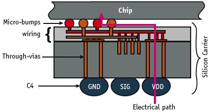
Figure 1. Silicon carrier and its electrical elements
2. Silicon carrier
An appreciable amount of papers describing fine pitch and through wafer interconnects in silicon substrate have been published over the last five years, focusing primarily on a 3D stacking of chips that strives to achieve greater than 100% packing efficiency for portable electronics and dense memory applications. Several papers have been published recently by IBM Research that introduced the silicon carrier technology for a wide range of 2D and 3D product applications and presented detailed descriptions of its key technology enablers. In its most basic form, the silicon carrier is a silicon substrate that has fine pitch I/Os and high speed wiring on one side, a typical C4 solder bump on the other side and through-vias that connect the two sides (Figure 1).
2.1 Electrical elements
From an electrical perspective, a path traversed by a signal or power I/O on the silicon carrier involves four elements: (i) micro-bump; (ii) wiring; (iii) throughvia; and (iv) C4. Depending on the application, the silicon carrier can play the role of a first-level package to an entire system ready to be attached to a board. As a result, its electrical elements may be required to conform to a wide range of specifications that can vary significantly from what are considered to be ‘normal’ on chip and package specifications.
Examples of such a wide range of specifications include signal net lengths ranging from a few hundred microns to tens of millimeters, bus frequencies ranging from a few hundred megahertz to tens of gigahertz, application dependent signal and power distribution schemes, micro-bump and through-via pitch ranging from 225um to less than 50um, or through-via (and consequently silicon carrier) height ranging from 300um to less than 50um. As will be discussed in Section 3, thorough characterization of silicon carrier has shown that it can be designed to meet such divergent requirements. The challenge, however, lies in developing electrical models that can easily conform to these varying requirements and are simple enough to be integrated in EDA tools.
2.2 EDA issues
Widespread usage of any new technology not only depends on the advantages it offers, but also on the ease with which it can be integrated or adapted within the framework of existing design tools. This integration enables the designer to fully assess the potential of the technology. Existing circuit and system simulators have already reached an exemplary level of sophistication in that they are capable of simulating multiple processor core interactions with hierarchical caches through a complex and dense network of signal/power/clock interconnects. The easiest and perhaps the fastest entry point for the silicon carrier within the existing EDA environment would be then to build on to this level of sophistication of EDA tools and develop representative electrical models of each one of the silicon carrier electrical elements so that they can be readily integrated within the tools as just another element of an already complex system. A signal or a power connection on the silicon carrier can be a combination of its electrical elements grouped into one of the four cases (see Figures 2a – 2d).
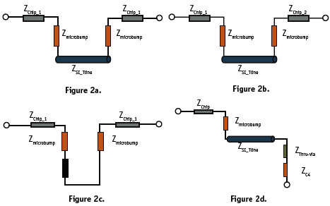
Figure 2. Electrical paths for signal and power distribution on silicon carrier and the elements involved
Figure 2a represents a case where it would be desirable to transfer some of the lossy on-chip wiring to relatively low loss wiring on the silicon carrier. This case advocating the concept of so-called ‘exterconnects’ can help mitigate performance limitations imposed by the longest interconnects on a chip in a cost effective manner. The path traveled by a signal in this case would involve a designated net length on chip originating from a source (Zchip1), a micro-bump (Zmicrobump) to exit the chip, an exterconnect (ZSi_Tline), a micro- bump (Zmicrobump) to reenter the chip and a designated net length on chip terminating on a sink (Zchip1).
Figure 2b represents a case where multiple homogeneous chips (i.e., all chips are of the same type such as Si BiCMOS) or heterogeneous chips (i.e., chips from different technologies such as Si CMOS and InGaAs optoelectronic components) are assembled onto the silicon carrier to form a system and are required to be interconnected. Such integration takes advantage of the planarity and ease of processability of the silicon substrate as well as its high density and high performance signaling capability – a combination of features that is not available in other technologies such as polymer-based organic or ceramic substrates. This can also represent a case where multiple units of a large chip (i.e., processor core and/or caches) are fabricated individually as smaller chips and then assembled tightly onto the silicon carrier using chip-to-chip placement distances of less than 100um to reformulate the function of a large chip, but as a result, avoiding problems associated with yielding large chips. Electrical elements involved in this case are very similar to what we see in Figure 2a (i.e., a signal goes through two microbumps (Zmicrobump) and net length (ZSi Tline). The only difference is that the line terminates on a second chip involving a sink element on that chip (Zchip_2).
Figure 2c involves a chip accessing passive components such as a resistor, an inductor or a capacitor that may be embedded within the silicon carrier. In many applications, the passives within the silicon carrier are desired because they can be placed very close to the chip. Silicon carriers with micro-bump height as small as 8um have been reported. Such close proximity can significantly enhance the effectiveness of the passives in improving chip performance. For example, silicon carriers with decoupling trench capacitors having the capacitance of 2.5-2.7uF/cm2 have been designed and characterized. This high density of capacitance and its close proximity can provide low inductance decoupling for high performance chips. In this case an additional element called Zpassive is introduced.
Finally, Figure 2d (p37) represents a situation where a signal or power is traversing the silicon carrier as a result of traveling between the chip and the ‘outside world.’ Besides the micro-bump and a net length, the through-via (ZThru_via) and C4 connection (ZC4) are involved in this situation.
These four cases represent the most basic uses of silicon carrier in computer systems. There could be other variations, but at the minimum, those variations would involve a sub-set of the electrical elements discussed in Section 2.1.
The most important characteristic of Figure 2a – 2d is that, electrically, each one of the silicon carrier elements can be modeled similar to an on-chip component once its parasitic R, L, C are characterized. The micro-bump and through-via can each be modeled in a similar way to an on-chip inter-metal via, the passive elements can be modeled as on-chip passive components and the exterconnects or signal lines can be modeled with simple modification as on-chip signal nets. These elements can then be made part of a design and simulation kit. This would allow the designers building a chip or an architect trying to analyze the system to make these components an integral part of the design just like CMOS devices and back-end metal levels.
There are several trade-offs that an on-chip designer may face in choosing the silicon carrier technology. Clocking and clock distribution can be a challenge in applications where a large die is only physically partitioned into smaller chips and coherent clocking is still expected. This can be mitigated by architecting the large die as a system of small chips. If the system uses a silicon carrier, inherently, it cannot be tested without a silicon carrier. This might pose a challenge in the cases where wafer level full functional testability is required. An efficient solution to this problem is currently being investigated at IBM Research. Because of close placement of chips on the silicon carrier, heat removal may become an issue for chips dissipating large amount of power. However, the latest developments in thermal interface materials and copper heat sinks coupled with micro-channel liquid cooling assure heat removal capability of greater than 300W/cm2.
Additionally, chips that are assembled on the silicon carrier can be thinned down to the same thickness using well-developed wafer thinning technologies. This would provide a planar surface across the chips that could then be used to attach a heat sink. In addition to these, a designer will face a multitude of performance tradeoffs while designing the silicon carrier electrical elements. These trade-offs are discussed in the next section.
Out of the four basic electrical elements of the silicon carrier mentioned in Section 2.1, the parasitics of three of them are analyzed in Section 3. The significance of these elements in enhancing the overall system performance is also discussed. C4 connections have been extensively characterized over the last 40 years and are not discussed in Section 3. A fairly recent handbook (Area Array Interconnection, Putlitz, K. and Totta, P. (editors), Springer Publications) captures much of its characterization.
3. Characterization of silicon carrier electrical elements
3.1 Micro-bumps
Micro-bumps are the primary interface that is traversed every time data and power are exchanged between the chips and the silicon carrier. For high performance systems, it is essential to maximize the density of micro-bumps and minimize the electrical parasitics. A larger number of micro-bumps, if available, can be used as signal I/Os to increase the width of the bus between two chips or between a chip and its memory caches and, as a result, significantly increase overall bandwidth of the system. They can also be used as power I/Os in a power distribution grid to substantially reduce DC drops in power grids. The micro-bumps would be deemed useless if their parasitics negated any of the aforementioned gains in signal or power distribution. Hence, it is equally critical to minimize the electrical parasitics of the micro-bumps; the ultimate limit of which would be to reach a point where micro-bump parasitics become comparable to that of an on-chip back-end-of-line (BEOL) via.
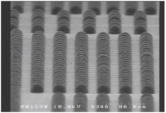
Figure 3. Silicon carrier with 50 um pitch micro-bumps
Area array micro-bumps with nominal diameters of 50um and 25um and pitch of 100um and 50um, respectively, have been fabricated (see Figure 3) on the silicon carrier and electrically characterized. DC contact resistances equaling 14m? and 17m? were obtained for 50um and 25um micro-bumps, respectively. By comparison, the DC contact resistance of a typical 100um diameter C4 bump is about 5m?. The resistances include the contribution of a pad that lies underneath the micro-bump. The absolute resistance of a micro-bump is higher than a normal C4. But because the density of micro-bumps is higher than that of typical C4 having 100um diameter and 200um pitch, the equivalent resistance of micro-bumps per unit area is less than that of C4. As a result, for a fixed current density, the DC power drop in the micro-bumps will be lower than C4. For example, a 4X4 array of 16 50um pitch micro-bumps can replace one 200um pitch C4 bump. Not only is the effective area serviced by a power micro-bump reduced by a factor of 16 (yielding a shorter connection path between a source and a sink), but total current within that area is also reduced by a factor of 16. These two combined achieve reduced DC drops in power grids.
Micro-bumps with 50um diameter and 100um pitch have been characterized up to 40GHz using transmission line test macros in and with the performance of time and frequency domain measurements. Additional delay of 6ps and less than 0.5dB of transmission losses were measured when going through a 50um diameter micro-bump. For clock frequencies up to 10GHz, 6ps is a small fraction of the clock cycle and a negligible addition to inter chip communication links at these frequencies. The delay and the losses are expected to reduce as the micro-bump diameter and its respective pad is scaled down to smaller dimensions. Non-uniform current crowding and spreading resistance play a significant role in determining the electrical parasitics of microbumps and make it difficult to deduce a simple scalar model that predicts the impact of micro-bump dimension scaling on its electrical parasitics. The derivation of such a model is a subject for future investigation. However, AC/DC characterizations of 50 and 25um micro-bumps that have been performed thus far are sufficient for constructing micro-bump elemental models and making them discretely available within EDA tools.
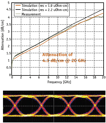
Figure 4. Measured and simulated attenuation per unit length for differential microstrips and corresponding eye (7mm microstrip line EYE at 20Gbps)
3.2 Wiring
The wiring on the silicon carrier is one of the most versatile elements. It has to conform to a wide range of specifications such as 1-20GHz operational frequency or 1-50mm signal net lengths. This variance in frequency and net lengths is further complicated by the additional requirement of link loss budgets that specify transmission and return losses on interconnects. In general, the wiring levels on the silicon carrier are similar to top most on-chip BEOL levels. The main difference is that silicon carrier wires can be designed to be 2-3X thicker than BEOL wires and, as a result, have lower transmission and power losses. High fidelity signaling and effectively lower cross talk can be achieved by carefully shielding the signal lines in-plane and/or out-of-plane through various signaling schemes. Problems arising from via blockages and wire limited routing can also be alleviated to a certain degree by making use of silicon carrier wires and designating them as a separate tier or an extension of on-chip wiring levels.
To characterize the high speed signal performance of wires in silicon carrier, two separate test sites that included hundreds of test macros covering the wide range of operating frequencies, net lengths, and signaling schemes were designed and measured in time and frequency domain.
One test site focused on the design of a high speed electrical-optical transceiver operating at an aggregate bandwidth of 1Tbit/sec. This test site explored high speed differential microstrip lines that could operate in the 10-20GHz frequency range with less than 5dB/cm transmission losses. Three levels of wiring (one each for power, ground and signal) were fabricated on the silicon carrier. The differential microstrip transmission lines were designed with a line width of 4.5um, space of 15um and a channel-to-channel spacing of approximately 100um. As shown in Figure 4, the signal attenuation on such lines was measured to be approximately 4.3dB/cm at 20GHz and relatively wide eye openings were measured at a data rate of 20Gbps.
The second test site focused on the design of a high bandwidth computing node. This test site was designed to achieve maximum bisection bandwidth by maximizing the signal wiring density that could operate in the 1-10GHz frequency range. The impact of high wiring density on signal integrity was also explored by studying different types of signaling schemes (Figure 5).
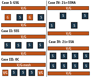
Figure 5. Silicon carrier signaling schemes
Case I examined the effect of in-plane and out-of-plane shielding on signal performance. Case II represented a typical packaging situation where signal levels are sandwiched between power and ground levels. Case III represented a wire limited chip where power, ground and signals may be forced to share a level. And finally, case IV represented a plane-pair scenario. Both the line length and line density (i.e., width, space and pitch) were varied for each one of the four cases and the impact of those variations on signal transmission and integrity was examined by performing time delay transmission (TDT) and far end noise (FEN) measurements in time domain as well as s-parameter measurements in the frequency domain.
Complete analysis and description of the results is beyond the scope of this paper but a small subset of results is shown in Figure 6. The figure plots the FEN and bisection bandwidth on y1 and y2, respectively, for a number of cases labeled on the x-axis. The bisection bandwidth is a factor that is obtained by dividing the 3dB frequency of the line by its minimum wiring pitch. Bisection bandwidth (having units of GHz/um) represents a metric that should be maximized in order to achieve the highest possible bandwidth on the silicon carrier. For example, consider a case where signal A is operating at 10GHz and a wiring pitch of 50um and signal B is operating at 2GHz and wiring pitch of 4um. For a bisection measuring 1mm across, signal A with bisection bandwidth of 0.2GHz/um results in 200Gbps bandwidth whereas signal B with bisection bandwidth of 0.5GHz/um results in 500Gbps bandwidth. Hence, the normalization of signal frequency by its wiring pitch is helpful in readily assessing signal performance of silicon carrier wiring for applications desiring high computing power. For cases plotted in Figure 6, signal lines could be optimized to obtain FEN values between 1.2 to 35% and simultaneously, this would correspond to a bisection bandwidth ranging from 1.5 to 6.5GHz/um.
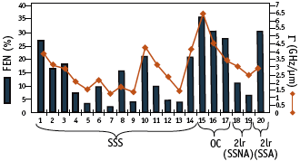
Figure 6. Bisection bandwidth and FEN values for a subset of signal lines on siliconcarrier
If the FEN budget is given and if maximum bandwidth is desired, a designer would pick a signal case yielding the highest bisection bandwidth. Depending on the design of these signal nets on silicon carrier, their characteristics range from mostly RC to LC to anywhere in-between. These can therefore be modeled as lossy transmission lines and used in EDA tools. A distributed RLGC representation of these lossy lines also provided very good agreement with the measured results.
3.3 Through-vias
Through-vias bring the power and signals from the ‘outside’ world and supply them to the chip using the wiring on the silicon carrier. The inductance and the current carrying capacity of a through-via are important parameters that aid in efficient power distribution. Low inductance is highly desirable to minimize LdI/dt voltage drops in power delivery networks for ASICs or microprocessors.With rapid increases in on-chip power dissipation, the through-vias are also required to withstand higher current flow. A through-via that has an annular column of metal with a silicon post intact inside the annulus has been reported to be a reliable structure. The annulus of the through-via is filled with copper or tungsten conductor.
Depending on the type of application, the thickness of the annulus can range from 2-6um whereas its height can range from 50-200um. Because C4 solder bumps are used to connect the silicon carrier to the next level, the inner diameter of the annulus and the pitch are typically fixed at 50um and 225um, respectively.
The inductance of two different heights of silicon carrier through-vias was measured using a vector network analyzer. The per unit length inductance of a through-via was measured to be approximately 0.15pH/um, the smallest reported value for through-vias in silicon. This value of inductance was observed to scale linearly with the height of a through-via. For example, the measured inductance for a 185um tall through-via was 41pH and that for a 271um tall through-via was 63pH. The DC resistance of a through-via was also measured and depending on the metal fill it was found to be within 0.16-0.25m?/um. Preliminary measurements aimed at understanding the maximum current carrying capacity of a through-via showed that as much as one amp was passed through a via prior to the failure of peripheral wiring used in the test setup. The low inductance, low resistance, high current carrying capacity coupled with high density microbumps and low loss (DC power) electrical wiring provide an effective savings on total power dissipation within the supply grid and in turn, aid in increasing overall system performance.
To ascertain how much additional delay was incurred as a result of sending a signal through a through-via, TDT measurements were made on samples with and without through-vias. Figure 7a and Figure 7b show the TDT results for two separate macros which conclusively establish a negligible 3dB delay of 0.75ps for traversing a through-via. The through-via in this case was filled with tungsten and its height was 60um. Derivation of per unit length resistance and inductance values for through-vias makes it much easier to develop a representative RLC model that can be scaled based on the geometry of the through-via and integrated within EDA tools.
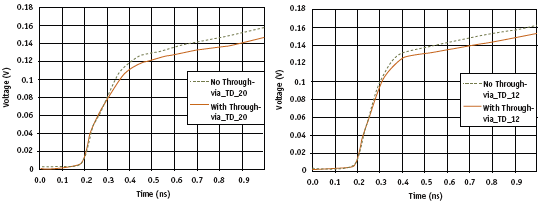
Figure 7. TDT measurements of silicon carriers with and without a through-via show a 3 dB delay of 0.75 ps
4. Conclusion
We have considered the electrical characterization of key electrical elements of the silicon carrier being developed at IBM Research and the significance of those elements in enhancing the overall system performance. Some methodologies that may allow silicon carrier technical elements to be easily integrated within existing EDA tools are also discussed. In particular, those elements have the following electrical characteristics:
Micro-bumps
- DC resistance ? 14-17m?
- -3dB delay ? 6ps (including pads)
- Less than 0.5dB loss up to 40GHz
- Current carrying capacity in excess of 100mA wiring
- f-3dB for 2.5mm line lengths ? 6.5 to 11.7 GHz
- Far end crosstalk range 1.2 to 39%
- Differential microstrip T-lines up to 20Gbps with 4.5 dB/cm attenuation Through-vias
- Inductance ? 0.15pH/um
- DC resistance ? 0.16 – 0.25m?/um
- -3dB delay ? 0.75ps
- Estimated current carrying capacity ƒ 1.0A
These values and general characterization can be used to form the electrical models which can be integrated within existing EDA tools. This would permit designers to fully simulate a system with silicon carrier and optimize its impact on overall system performance.
Acknowledgements
The author would like to thank Alina Deutsch, Keith Jenkins and Christopher Surovic at IBM Research for their support in measuring the performance of wiring levels on the silicon carrier. The author is also grateful to the members of the silicon carrier team whose prior publications on this topic have informed this paper. Due to pressures of space, the full set of references for this article can be found online at www.edatechforum.com. This work has been partially supported by Maryland Procurement Office.
IBM T. J.Watson Research Center
1101 Kitchawan Road
Yorktown Heights
NY 10566
USA
www.ibm.com
