Reducing PCB design cycle by 60%
The PCB design team on Alcatel Shanghai Bell’s recently introduced A7510 Media Gateway product was given only seven weeks to complete its task against an original estimate of 13 weeks. The article describes how the team added new members and adopted a concurrent design strategy to not merely meet but beat the tightened deadline.
Specific lessons learned included:
- the value of assigning team members according to their expertise rather than simply the next stage that required design;
- the importance of using EDA tools that have been specifically architected to enable collaborative, concurrent design;
- the structure needed for effective design management; and
- the need to match computational resources to the way the design cycle has been structured, once a concurrent strategy is chosen.
Design infrastructure
Alcatel Shanghai Bell (ASB) is the first foreign-controlled telecommunications company in China, with Alcatel-Lucent owning 50%-plus-one-share and Chinese shareholders holding the remainder. The company provides end-to-end telecommunications products and services in application areas such as fixed/wireline, mobile/wireless, broadband access, optical, multimedia and general networking.
ASB has its own R&D center, which also has access to and works with Alcatel-Lucent’s global technology pool. ASB can thus develop original technologies both for use in China and for export to Alcatel’s customers worldwide.
ASB comprises several Product Business divisions. Rather than duplicate various types of design expertise in each, the company has the Common Competence Center (CCC). This is ASB’s overarching organization for research, development and implementation in the PCB, FPGA, mechanical, and EMC/EMI design segments. All PCBs are therefore designed by the appropriate part of the CCC. In addition, the CCC provides all EDA tool support for the Product Business divisions.
The project
The product that forms the basis for this case study is not only complex—requiring the use of both leading-edge electronics technology and state-of-the-art manufacturing techniques—but also had to be designed and delivered to a tighter deadline than any project previously undertaken by ASB.
The high-capacity A7510 Media Gateway addresses key functions required for next-generation network (NGN) and IP multimedia subsystem (IMS) architectures. It provides any-to-any media switching and interworking for circuit and IP ports for voice, fax, and data. It also provides PSTN migration and new IP services in both the metro transit and the local access layers of Alcatel-Lucent’s IMS products as well as for any multi-vendor NGN.
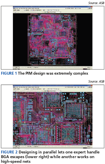
For this particular project, the CCC’s PCB team was responsible for the design of a package interface module (PIM) board. The complexity of the PIM matched that of the overall product (figure 1). The PIM comprises 16 layers, 3,823 nets, and 67,023 individual traces on a 310x330mm board. The board hosts 5,533 separate components and has a total pin-count of 20,206. In addition, during design more than 70% of the nets had specified high-speed constraints and 15% of the nets used differential pairs. PIM features include 800MHz DDR-II RAM, 1.25Gbps SERDES, Gigahertz Ethernet, SPI 4.2, 800MHz QDR SRAM, 777.76MHz SBI336S serial bus, and 800MHz HyperTransport.
Such a project typically requires the combination of three elements: talented designers, excellent design tools and plenty of design time. Our team had two—time to market was heavily constrained. PCB design manager Wei Li calculated that using her two lead designers, it would take 13 weeks to design the PIM. However, the Product Business division needed the job done in seven weeks.
Designing in parallel
With time at such a premium, attention turned to the two components over which Wei Li still had some control: people and tools. She decided to take advantage of the fact that the CCC held four seats for Mentor Graphics’ XtremePCB product, which is specifically architected to enable real-time collaborative design, and therefore assigned four more engineers to join the core team of two. The objective was to introduce some engineering redundancy so that each seat on the tool was ‘hot’ for as long as possible. In this way, the team would seek to work within the seven-week time budget by using a parallel and concurrent design strategy.
Obviously, this presented significant challenges in terms of the scheduling and management of the design flow. There is plenty of scope for problems when you have six talented designers working on the same project across just four seats (e.g., scheduling conflicts; deciding who has the lead role and when; task assignment; and handling ‘creative’ egos).
With up to four designers working on the same design at the same time, all six engineers had to bond together into a ‘total’ team. The good news here was that, having collaborated for years and understanding one another’s capabilities, the group was able to accept and adapt to the new working model quickly and easily.
The two principal designers kept their two seats active, coordinating the overall project design. Subsections were then individually assigned. As the other engineers had time or as a seat opened, each rotated in or out so that work was continuous.
However, in addition to giving portions of the project to designers as they became available, we sought to take advantage of the various team members’ areas of expertise. For example, principal designer Hui Wang was identified as the right person to focus on the DDR-related aspects of the design while principal designer Lifan Sun was seen as being best placed to concentrate on the ball grid arrays as well as PCI, HyperTransport and SPI buses. We found that when these and other team members were assigned on this basis, their individual design tasks were generally completed ahead of schedule. We therefore believe that this is the most efficient way to achieve concurrent design with such a number of engineers.
As the project moved forward, the team became more and more optimistic about meeting its deadline. The XtremePCB software allowed us to work quickly but creatively—engineers in each of the seats could work within their areas of expertise at the same time on the same PCB (figure 2).
Tasks progressed with more ease than we had originally forecast. Thirteen weeks soon looked like an embarrassingly comfortable schedule, and it became increasingly apparent that the team might even beat the reduced seven-week target. Clearly productivity was way up.
One of the most unexpected discoveries was how significantly productivity increased as the team added each new designer. In the past, we found adding an engineer to a project gave about 30% of an ‘engineering resource’ increase in productivity and in terms of time-to-completion. With the new software, we found adding an engineer contributed 70% of an ‘engineering resource’ increase.
What in the beginning had been expected to be an intense 13-week process, had been cut to seven but was ultimately completed in just five weeks: 60% under the original estimate for design time.
Hui Wang summed the team’s impressions: “Without collaborative, concurrent software like XtremePCB, we couldn’t have completed such a complex PCB design in five weeks, even if we’d worked day and night.”
Moving forward
Nevertheless, as always happens during the first use of any product or design flow, the team did identify some areas where further improvements would be possible on any subsequent project. These boiled down essentially to modifications across three topics.
- Computational resources—Making sure that the PC platform is powerful enough to deal consistently with concurrent design sessions, and that it has ample memory.
- Assign blocks explicitly—Efficiency is maximized if different blocks and different layers are assigned to designers in advance rather than on-the-fly.
- Reserve first—Perhaps most importantly, it is well worth having the agreement of all designers that one layer will be ‘reserved’ at the very beginning of the project. That layer can be then used to route those nasty few traces that always crop up at some stage.
Alcatel Shanghai Bell Co., Ltd.
388/389 Ningqiao Road
Pudong Jinqiao
Shanghai
201206
P.R. China
T: +86 21 58541240
W: www.alcatel-sbell.com.cn (currently Chinese language only)
