Power analysis for efficient power planning
As designs grow larger and process technologies continue to shrink, power becomes an increasingly important design consideration. When designing a printed circuit board (PCB), the power consumed by a device needs to be accurately estimated to develop an appropriate power budget and to design the power supplies and cooling system. The PowerPlay power analysis technology, part of Altera’s Quartus II software, assists such with power planning.
Power planning
Power analysis is directed towards two essential power planning requirements: thermal planning and power supply planning. For thermal planning, the designer must ensure that the cooling solution is sufficient to dissipate the heat generated by the device. In particular, the computed junction temperature must fall within normal device specifications. For power supply planning, the designer must ensure adequate current to support device operation on the board.
The two requirements are closely related because most of the power supplied to the device is dissipated as heat from the device itself. However, in some situations, these requirements are not identical. For example, when the designer uses terminated I/O standards, some of the power drawn from the FPGA’s power supply is dissipated in termination resistors, rather than in the FPGA.
The PowerPlay power analysis tools in Altera’s Quartus II design software give designers the ability to estimate power consumption from early design concept through design implementation.
Factors affecting power consumption
The factors affecting power in FPGAs are device selection, environmental conditions, resources used by design and signal activities. Understanding these factors allows designers to effectively use the PowerPlay power analysis tools.
Device selection
Different device families have different power characteristics. Many parameters affect device family power consumption, including choice of process technology, supply voltage, electrical design and device architecture. For example, Altera’s Cyclone II FPGA family architecture was designed to consume less static power than its high-performance, full-featured Stratix II FPGA family. The choice of device package also affects the device’s ability to dissipate heat. This can impact the choice of the cooling solution required to meet junction temperature constraints. Finally, process variation can affect power consumption. It primarily impacts static power, since sub-threshold leakage current varies exponentially with changes in transistor threshold voltage. As a result, it is critical to consult device specifications for static power and not rely on empirical observation. Process variation mildly affects dynamic power.
Environmental conditions
Operating temperature primarily affects the static power consumption of the device, increasing junction temperature and resulting in increased static power consumption. The thermal power and cooling solution used must result in the device junction temperature remaining within its maximum operating range. The main environmental parameters affecting junction temperature are the cooling solution and ambient temperature.
Air flow
This is a measure of how quickly heated air is removed from the vicinity of the device and replaced by air at ambient temperature. This can either be specified as ‘still air’ when no fan is used or as the linear feet per minute rating of the fan used in the system. Higher air flow decreases thermal resistance.
Heat sink and thermal compound
A heat sink allows more efficient heat transfer from the device to the surrounding air. The thermal compound that interfaces the heat sink to the device also influences the rate of heat dissipation. The case-to-ambient thermal resistance (CA) parameter describes the cooling capacity of the heat sink and thermal compound employed at a given airflow. Larger heat sinks and more effective thermal compounds reduce CA.
Ambient temperature
The junction ambient temperature of a device is equal to: TJUNCTION = TAMBIENT + PTHERMAL JA where JA is the total thermal resistance from the device transistors to the environment, having units of degrees Celsius per Watt. The value JA is equal to the sum of the junction-to-case (package) thermal resistance (JC) and the case-to-ambient thermal resistance (CA) of the cooling solution.
Design resources
The design resource used greatly affects power consumption.
- Number, type and loading of I/O pins
Output pins drive off-chip components, resulting in high-load capacitance that leads to a high dynamic power per transition. Terminated I/O standards require external resistors that generally draw constant (static) power from the output pin. - Number and type of logic elements, multiplier elements and RAM blocks
A design with more logic elements (LEs), multiplier elements and memory blocks tends to consume more power than a design with fewer such circuit elements. Also, the operating mode of each circuit element affects its power consumption. For example, a digital signal processing (DSP) block performing 18×18 multiplications and a DSP block performing multiply-accumulate operations consume different amounts of dynamic power due to different amounts of internal capacitance being charged on each transition. Static power is also affected, to a small degree, by the operating mode of a circuit element. - Number and Type of Global Signals
Global signal networks span large portions of the device and have high capacitance, resulting in significant dynamic power consumption. The type of global signal is important as well. For example, Stratix II FPGAs support several kinds of global clock networks that span either the entire device or a specific portion (e.g., a regional clock network covers a quarter of the device). Clock networks that span smaller regions have lower capacitance and, therefore, tend to consume less power. In addition, the location of the logic array blocks (LABs) driven by the clock network can have an impact; Quartus II software automatically disables unused branches of a clock network to save power consumption.
Signal Activities
The most important factor in estimating power consumption is the behavior of each signal in the design. The two vital statistics are the toggle rate and static probability.
The toggle rate of a signal is the average number of times that signal will change its value per unit of time. The units for toggle rate are transitions per second, and a transition is a change from 1 to 0 or 0 to 1. The static probability of a signal is the fraction of time that the signal will be logic 1 during the period of device operation being analyzed.
Power Analysis Tools
Designers can estimate power at different stages of the design cycle. Depending on the design cycle stage and the accuracy of the estimation required, designers can either use the PowerPlay Early Power Estimator spreadsheet available from the Altera web site or the PowerPlay Power Analyzer tool in the Quartus II software.
PowerPlay Early Power Estimator
Because FPGAs provide the convenience of a shorter design cycle and faster time-to-market, the board design often takes place during the FPGA design cycle. This means power planning must happen before the FPGA design is complete.

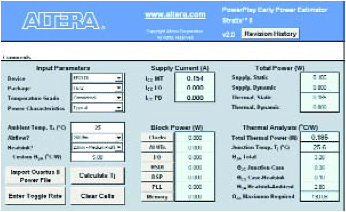
Figure 1. Early Power Estimator
If the FPGA design has not yet begun or is not complete, an estimate of the power consumption for the design can be made using the Early Power Estimator spreadsheets (see Figure 1). Separate spreadsheets are available for each device family.
PowerPlay Power Analyzer
When the FPGA design is complete, accurate device power consumption can be estimated with the PowerPlay Power Analyzer tool in Quartus II software. Run the Power Analyzer after synthesis and place-and-route are completed for detailed information on design implementation and high-quality power estimates.
PowerPlay Power Analyzer Flow
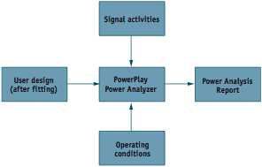
The PowerPlay Power Analyzer supports accurate and representative power estimation by letting designers specify the important factors affecting power. Figure 2 illustrates the high-level Power Analyzer flow.

Figure 2. High-level Power Analyzer Flow
Signal Activities Data Sources
The Power Analyzer provides a flexible framework for specifying signal activities, which reflects the critical importance of using representative signal activity data during power analysis. The data sources are simulation results; user-entered node, entity and clock assignments; user-entered default toggle rate assignment; and vectorless estimation (available for Altera’s Stratix II, Cyclone II FPGA and MAX II CPLD families).
The Power Analyzer lets designers mix and match signal activity data sources on a signal-by-signal basis. Using simulation results is the most accurate way to generate signal activities. This, in turn, is used to accurately estimate the power consumed by the device during operation. The PowerPlay Power Analyzer reads the results generated by the Quartus II simulator and other third-party EDA simulators. This flow provides the highest accuracy, as all node activities reflect actual design behavior, provided that supplied-input vectors are representative of typical design operation.
Operating Conditions
Operating conditions can be specified, including device power characteristics (typical or maximum), environmental conditions and junction temperature. The Power Analyzer can automatically compute the junction temperature based on the specified ambient temperature and cooling solution. Designers may select from a prepared list of sample cooling solutions. For a more accurate analysis, designers can directly enter the thermal resistance of their exact cooling solution.
Power Analysis Optimization
The PowerPlay Power Analyzer provides a comprehensive power consumption report designers can use to optimize thermal power dissipation on a block-type or design-hierarchy basis. The report is divided into different sections for detailed information:
- The ‘Summary’ section provides an estimated total thermal power consumption of the design. This includes the dynamic power, static power, and routing power consumption.
- The ‘Settings’ section shows the design’s Powerplay Power Analyzer settings information. This includes default input toggle rates, operating conditions and other relevant setting information.
- The ‘Operating Conditions Used’ section provides device characteristics, voltages and cooling solution, if any, that were used during the power estimation.
- The ‘Thermal Power Dissipated by Block’ section shows estimated thermal dynamic power and thermal static power consumption categorized by atoms, providing designers with estimated power consumption for each atom in their design.
- The ‘Thermal Power Dissipation by Block Type’ section provides the estimated thermal dynamic power and thermal static power consumption categorized by block types.
- The ‘Thermal Power Dissipation by Hierarchy’ section shows an estimated thermal dynamic power and thermal static power consumption categorized by design hierarchy, then sub-categorized by the dynamic and static power used by the blocks and routing within that hierarchy. This is very useful in locating design modules that consume high power and using this information to optimize the design for low power consumption (Figure 4).
- The ‘Power Drawn from Voltage Supplies’ lists the power drawn from each voltage supply.
- The ‘Confidence Metric Details’ section provides information about the quality of the signal activity data sources.
- The ‘Signal Activities’ section lists toggle rate and static probabilities assumed by power analysis for all signals with fan-out and pins.
Conclusion
Advances in semiconductor technology have led to smaller transistor dimensions and devices with higher densities, higher performance, low voltage and low power dissipation. At the same time, designs have become larger and more complex, causing devices to consume more power. This makes it vitally important to accurately estimate power consumption for a design. The PowerPlay power analysis tools in Altera’s Quartus II design software enable designers to do just that: estimate power consumption from early concept through design implementation.


