Portable multimedia SoC design: a global challenge
Today more than ever, the difference between design success and failure resides in engineers’ ability to master all critical design factors at once. Meanwhile, systems-on-chip (SoCs) represent a multidisciplinary challenge that spans the entire flow from architecture through design to test and finally mass production. For portable applications in particular, SoCs present especially stringent constraints that challenge the ability of any organization to fully master its industrialization capabilities and push concurrent design strategies to new limits. Only the combination of a well thought-out architecture, best-practice design techniques, a high level of understanding of the manufacturing constraints, and excellent logistics can deliver the devices that can be produced to the volume requirements of the cellular phone industry. This paper describes how these challenges have been addressed by STMicroelectronics in the design of its family of Nomadik multimedia application processing engines. It specifically focuses on a third generation part, the STn8815S22, where the integration capabilities of silicon technology were coupled with those of system-in-package design to produce an extremely compact and effective SoC for portable multimedia applications.
Since the term system-on-chip was coined, a crazy loop between the exploitation of finer silicon geometries and the integration of new features on a single die has continuously gained speed. The scale of the task faced by SoC design teams is increasing at a greater rate than that of the products’ sophistication and it is seldom fully supported by an adequate off-the-shelf EDA solution. Overall, the shrinking rates of product development time and that during which new EDA environments can be qualified and introduced add complexity and risk. This subverts one traditional R&D goal, whereby organizations strive for predictability and reasonable stability in the development of their design environments and practices. Faced with forces that inject such complexity, STMicroelectronics (ST) has aimed to bring more simplicity to its strategies for architectural definition and design. How it has done so is illustrated here with reference to challenges presented during the development of a recent addition to the Nomadik multimedia application processing engine family, the STn8815S22 SoC (Figure 1). It is a third-generation Nomadik device and is packaged together with flash and DDR master storage memory.
Architecture
Start it simple to keep it simple. This is the key philosophy that guides the architectural definition of all components in the Nomadik family. Being able to run high performancemultimedia applications off a battery is neither a straightforward nor a natural process.Nomadik silicon specifically addresses the complex requirements of selective and variable levels of battery performance through a sophisticatedmultiprocessing structure that stands on a central processing unit and a set of smart accelerators implementing digital signal graphics functions. The clean way in which the bus interconnect andmemory hierarchies are defined as well as a clean division between the different components comprising the systemand the clear protocol under which they cooperate were vital to the successful design of the STn8815S22.
The massive set of models built around the Nomadik devices were also fundamental contributors to ensuring simplicity in implementation and predictability of results. Transaction-level and bit-true models provided tools for both the chip’s conception and the environment in which the SoC’s hardware and software were verified.
A further benefit of the selected architecture was that it enabled Nomadik SoCs to cope more easily with ECOs. The STn8815S22 underwent several hundred change requests over the course of its design life. Design practices at all levels strongly contributed to making it possible to meet these, but having a clean and simple architecture made changes simpler and more practical to achieve, enabling the introduction of new hardware features late in the design cycle.
Design
There is typically little flexibility to be had when you are designing an SoC for performance under huge power consumption constraints. Conventional RTL design capture was used to achieve devices targets but, as will be seen numerous times over the course of the project, the human factor (i.e., the skills, ability and preparation of the engineers) was the most important difference. The chip’s physical design certainly was a big challenge. The need to meet aggressive performance targets within minimal area and power forced the team to use the available tools in innovative and creative ways.
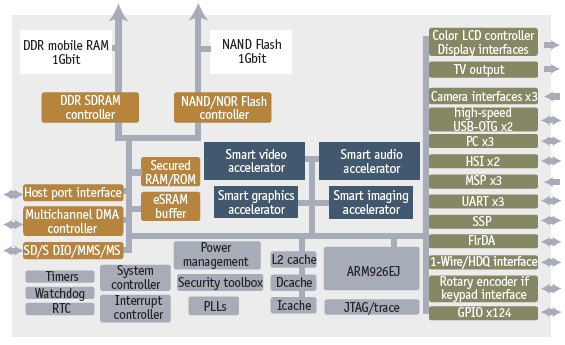
Figure 1. STn8815S22 block diagram
Constraints underwent multiple iterations and refinements, and custom scripting was needed to augment what EDA tools could not provide. On several occasions, R&D versions of EDA tools were needed either to cope with the complexity of the chip or of some specific aspect that was a result of extremely aggressive power containment techniques. This experience emphasized the importance of solid and trustworthy relationships with EDA vendors.Without these relationships, their R&D contributions and quick reaction times would have been critically lacking.
The STn8815S22 makes greater use of power islands, compared with earlier Nomadik generations. The technique allows flexible and independent management of supplies to different portions of the SoC, and presented one of the most critical design constraints. The design structure you use to maximize the power efficiency of the SoC, depending on active use cases and configuration, can be a source of nightmares when the flow reaches physical implementation. Here again, co-operation with ST’s central research functions as well as with our EDA vendors resulted in the definition of a design flow and design practices that allowed us to successfully build the chip.
The massive use of hard macros for the critical intellectual property blocks in the design helped to further simplify the problem and bring us to the right trade-offs between area, efficiency, power, circuit speed, and speed of design. Breaking up the design into manageable pieces had a positive impact not only during physical design, but also during all other aspects of the SoC build, including verification. Design for manufacturability and test was another area that required great investment in techniques and expertise. The device had a large number of memories and of sequential elements that were distributed across different supply domains. This made it necessary to resort to using the known tools and techniques in different ways. Power island partitioning, in particular, required significant effort and attention during scan stitching as well as in the overall scan definition to avoid issues of IR drop on automated test equipment. Clock tree synthesis marks the start of a painful process for most complex SoC designs. For Nomadik, the use of power islands and hard macros, added to the natural complexity of the STn8815S22, raised the bar significantly higher than before. Aggressive techniques that exploited preferential routing, useful skew, scripting, and dedicated library techniques greatly helped us scale the challenge.
Verification
The increasing complexity of devices from generation to generation has intrinsically moved the verification challenge to ever higher levels with each SoC revision. Yet techniques and tools that reduce the risk of many common design faults and of unwanted side behaviors exist. Specman is the backbone tool for verification of the Nomadik family. Its library of tests is enriched with each generation so it provides a robust environment. It is paired with formal proof techniques and used at each stage of refinement during the design capture and physical implementation stages. This was the hardware- oriented verification environment used for the design of the STn8815S22.
However, these tools alone are not sufficient for verifying Nomadik designs, as the family consists of an optimized balance of hardware and embedded software. To address embedded software within our our SoC verification methodology, we need to make an early prototype of the SoC available in an appropriate format for use by software engineers.
Nomadik designs employ a dual path approach to this aspect of verification, based upon different levels of debug capability and a suite of cooperative tools to facilitate traffic between the SoC and the embedded software design teams. The SoC is mapped on Palladium emulators and this is complemented by an FPGAbased prototype to allow concurrent software development. The ability to expose the SoC design to embedded developers towards the beginning of the flow allows a massive number of indirect test patterns to be exercised on the design and gives the team opportunities to improve the speed and ease of programming of the device at early stages in the design and industrialization phases. These opportunities more than repay the investment in prototyping.
Validation
Prototype validationmarks the point when the design teamfaces the truth.All the assumptions, uncertainties, trade-offs and related issues that have arisen can finally bemeasured against actual silicon. Time-to-market – and thereby time-to-design – must today be shortened with every generation, leaving less and less time for proper modeling and amassing a thorough understanding of all the physical effects that emerge at each progressive geometry. One cannot take it for granted that EDA platforms and libraries will fully match the actual behavior of the silicon, especially in the case of designs that are among the first to use a new technology. Nomadik SoCs are among those produced by ST on the latest technologies, sometimes at the pre-qualification stage. Consequently, the family’s design teams have developed a special sensitivity to the need to cope with major allied uncertainties and applied them during the design of the STn8815S22.
Taking ‘just enough margin’ is not a valid paradigm anymore. Prototype validation provides a set of tools that finally correlate simulation results with actual silicon and enable a set of process tuning and process re-centering steps that optimize both device speed and power. The use of corner samples (i.e., silicon that is pushed by construction into corner conditions of process parameters) is fundamental during this phase.Material tested in extreme temperature and voltage conditions provides a full set of parameters and relative values that allow process centering to be completed. After the basic tests to demonstrate the SoC is ‘alive and kicking’, each Nomadik platform is integrated into its development kit. This comprises the PCB and the toolset for embedded software development. The PCB hosts and mimics a mobile multimedia product. The development tools, though based on standard solutions, are specifically tuned to allow concurrent debugging,monitoring, and profiling of all CPUs and DSPs inside the STn8815S22. The kit is distributed to a vast number of engineers inside Nomadik’s embedded software community, sister divisions within ST, third-party embedded software specialists, and end customers. All these groups contribute to the full validation of the functionality and performance of a Nomadik SoC as it moves towards final qualification.
Packaging
Packaging is growing in importance and influence with regards to product cost and performance. The STn8815S22 is a system-inpackage (SiP), with the package hosting both non volatile and dynamic memories alongside the SoC. Assembling and testing the devices presents logistical as well as technical challenges. Memories have far shorter shelf lives than than multimedia application processing engines. This forced the Nomadik team to establish processes that limit the need to re-qualify the STn8815S22 whenever a DDR or flash update is required; that keep tight control of the relative die; and that ensure final good stocks. This work was carried out in coordination with customers to minimize end-product qualification efforts.
Stacking several dice in the same package is also no trivial task, particularly given footprint constraints in today’s typical end products (especially today’s cellular phones).While package planar dimensions have long been expected to be minimal, package thickness is also becoming increasingly important as manufacturers aim to deliver more slimline, high-end handsets. Targeting minimal thickness naturally raises tensions with regards to techniques such as wire bonding and demands the use of techniques like flip chip.
Stacking devices also requires that special attention be paid to potential warping effects of the package substrate. The improper combination and sequencing of the dice inside the package can induce substrate distortions that make connections to the PCB unreliable, even impossible. Three different packaging solutions were designed for the STn8815S22 before an optimal stacking of the four dice it embeds was chosen. High speed interfaces and multiple internal and/or external connections also raise serious signal integrity (SI) issues for the design of the package substrate. Nomadik benefits from a proprietary STMicroelectronics package design kit that allows engineers to simulate SI and other effects (e.g., thermal hot spots inside the package) early in the design flow. This technique proved extremely effective on the STn8815S22 especially for the management of high speed interfaces such as that between the processing engine and the integrated DDR memory.
Engineering
The Nomadik product engineering team worked together with the design group to maximize test coverage, yield, and the effectiveness of failure analysis in case of returns. During the STn8815S22 test program development, particular attention was directed towards yield monitoring and yield improvement processes. Sustaining cell phone production rates requires state-of-the-art practices in this regard, but, as an SiP, the STn8815S22, faced the additional challenge of having multiple dice suppliers, some part of ST and some not.
Security management also poses multifaceted challenges. Each customer can ask for the SoC to be customized through embedded hardware security features. Each SoC is customized at test time, when a signature is added to enable proprietary embedded software to run on the machine.
Project management
We made reference above to the experience and ability of all the staff involved in Nomadik and how their effective co-operative effort was central to a successful implementation. As with almost all SoC design teams today, Nomadik’s R&D organization is distributed across several international sites and spans multiple time zones. Project organization, access to effective methods for communication, the selection of the right people, and a positive attitude towards all challenges were all fundamental components in the successful delivery of the STn8815S22.
More than 400 people worked on the device at different stages contributing to its design and the industrialization of the device. The efficient management of such a large multidisciplinary design team really did make the difference between success and failure.
STMicroelectronics
12, rue Jules Horowitz – B.P. 217
F-38019
GRENOBLE Cedex
France
T: + 33 4 76 58 50 00
W: www.st.com
