Parasitics: an old problem reaches new heights
The semiconductor industry faces increasing challenges in the design of complex systems-on-chip, and while some have sprung from new, only recently anticipated sources, others are, in fact, very familiar. Foremost among these are the interconnect delays caused by the increasing influence of parasitic networks. Parasitic inductance is also a growing concern.
The causes of parasitic effects are well understood, as they pull upon such fundamental concepts as resistance and capacitance and they function in very much the way of the RC network that EEs will have first encountered as students. However, how they are addressed at today’s level of complexity – particularly in cutting edge SoC designs – still raises many questions over methodology and how available tools should be deployed.
Process geometries continue to shrink: 90nm already seems like yesterday’s node and as we accelerate through 65nm, devices constructed at 45nm are already in production, while 32nm is fast approaching. These steps have opened up previously unimaginable opportunities for system-on-chip (SoC) development. Complex chips loaded with features enable advanced devices, such as digital cameras, music players and global positioning systems and, increasingly, those which integrate these and other functions in a single product. But these developments also create problems. The fact that we can now place billions of transistors onto a single piece of silicon is creating new challenges that must be overcome if we are to continue to benefit from smaller lithography nodes.
One of those challenges is not a new phenomenon. In fact, it has been present since the first electronic circuit was conceived. But its effects have largely been ignored for the majority of the IC industry’s history. However, as the relentless scaling of transistor dimensions continues, interconnect delay, introduced by parasitic networks, is now becoming a huge limiting factor for ultra deep submicron design.
First principles
There are relatively few electronic principles, but understanding them and harnessing their potential has created an industry that continues to influence the course of progress in so many ways. Two of those principles are resistance and capacitance and it is these fundamental properties that combine to create the problem of interconnect delay.
One of the simplest circuits known to any electronics engineering student is the RC network, used widely to modify the shape of a changing signal. The inherent resistive and capacitive properties of any conductor mounted on an insulator will naturally create both resistance and capacitance in that connection. It is these unavoidable properties that create parasitic networks; indeed they effectively create RC networks that slow down or distort rapidly changing digital signals. And RC delay is not the only phenomenon impacting performance. Parasitic inductance is also an emerging problem.
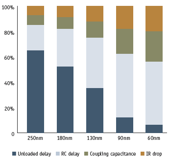
Figure 1. Parasitic effects increase dramatically as a share of limiting factors at smaller process nodes
Figure 1 is a diagram originally created by engineers at Synopsys which shows how parasitic networks have overtaken gate delay (unloaded delay) in becoming the primary limiting factor on performance. They are particularly apparent in long interconnects in an IC, due to their construction. As transistor scaling continues, interconnects must also scale, and as they reduce in width they increase in resistivity, while at the same time becoming more densely packed. All of this means that interconnects now exhibit even more unwanted RC features.
The answer may appear simple: avoid long interconnects. But as on-chip structures get smaller, ICs get larger in terms of gate density. While this enables highly complex systems to be created on a single chip, the process of designing an SoC has grown in complexity too.
It is no longer conceivable to design an SoC from scratch. SoC design now demands the use of complex and qualified building blocks of intellectual property (IP) that can be quickly and reliably imported into a design. Placing these IP blocks is not the main problem; the routing of signals between them presents as much if not more of a challenge. SoCs have effectively become wire-pitch limited and as more and more of the available silicon is needed for routing, the process of reliably connecting IP blocks is becoming more difficult.
Often, because IP is placed as mega blocks and not individual gates or transistors, connecting these blocks requires a relatively large number of contiguous connections that must all be routed long distances, running between other blocks and using all the available silicon space. It is this, as opposed to the comparatively short connections within IP blocks, that presents particular routing problems and impacts negatively on overall SoC performance. Figure 2 shows the massive impact of technology scaling on global wire delays.
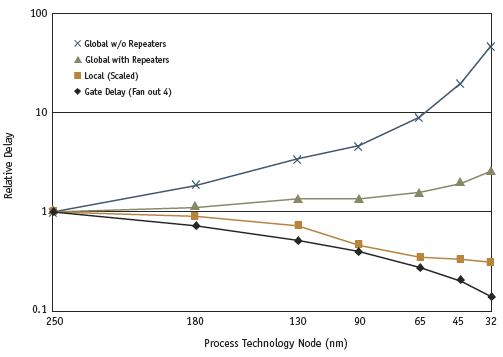
Figure 2. Delay trend for global wire connections at future process nodes
Routing problems cause signal integrity to suffer, particularly on critical connections. Therefore, signal integrity must be verified, under all operating conditions. At this point, parasitic inductance also becomes an issue.
Only when each and every connection between these complex blocks of IP is verified can the engineer have enough confidence in the entire chip design to sign it off for fabrication.With the cost of fabricating SoCs at 90nm and below becoming so high, making sure the design is right-first-time can prove to be the difference between commercial success and failure.
Parasitic delays and mutual inductance between signals caused by longer, thinner and more closely packaged interconnects are making verification increasingly difficult. Never before has the industry faced such pressures in the design phase and, as ever, engineers are turning to design tools in the search for some respite.
The problem today is that those tools have to undergo major improvement.With complex designs now comprising billions of layout polygons – all of which need to be accurately generated and verified – revisions and upgrades are required throughout the design flow.
Above and below RTL
For many years, and maybe for many more to come, designing complex ICs has and will continue to be achieved using an RTL (register-transfer level) approach. However, increasingly, the fact that we can put so many transistors on a single chip (albeit using IP building blocks) also demands more sophisticated approaches to that design which can take place above the RTL level.
We may all like the idea of being able to use electronic system level (ESL) tools to quickly define and verify complex SoCs. But – even though there has been a lot of progress in the past few years – a complete ESL flow for chip design continues to elude the market.
One of the problems lies with the compilation tools and how they manage the interface between the very high and abstract ESL view of the world and the traditional (backbone) RTL level that is used to run the detailed implementation.
It is at this stage that an automated path from high-level ESL descriptions to RTL (or even straight to gates) is needed. In addition to this translation, we also need automated tools (equivalence checkers) that can prove a lower level implementation (be it RTL or gates) matches the system level definition perfectly.
Using parasitic extraction tools, interconnect delays can now be modeled post-synthesis. Figure 3 shows a typical parasitic network schematic for a small circuit fragment. There can be potentially millions of networks such as this in a complex SoC design.
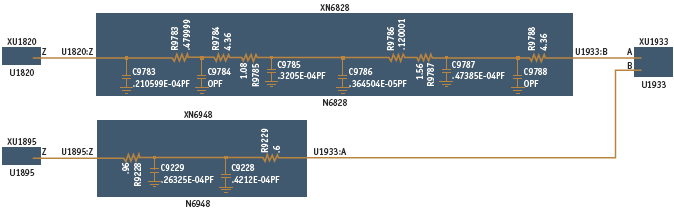
Figure 3. Visualization of parasitic networks
The schematic shows two logic gates driving two parasitic networks consisting of many RC components. This picture is automatically created, based on the parasitic network (e.g., a SPICE or DSPF netlist) generated by a parasitic extraction tool. Such extracted netlists can be used to accurately simulate the behaviour and timing of critical paths in a circuit. Advanced transistor-level visualisation tools, such as SpiceVision PRO from Concept Engineering, can read such network descriptions and show all the details of such parasitic networks, while built-in cross probing features allow each individual parasitic component to be located on the chip.
Interconnect Initiatives
At this year’s International Electron Devices Meeting (IEDM), NEC presented a paper that described a low-k dielectric which returns 11% less parasitic capacitance compared with other low-k dielectrics.
Based on a new silica-carbon compound (SCC) film, it effectively blocks copper (Cu) atom diffusion into the dielectric to establish a full-low-k (FLK) copper interconnect structure.
NEC claimed the process produces a dielectric constant (k) of just 35% of conventional low-k materials. Using the SCC film will also cut active power in interconnects and could be used at existing technology nodes as well as at 32nm.
A special stabilization process for the copper metal surface proved that the SCC film capping the copper lines maintained excellent insulation reliability, even after reducing the film thickness down to several tens of a nanometer.
This development is relevant because parasitic capacitance is also a source of active power consumption. The newly developed FLK Cu interconnect has a structure that ultimately makes it applicable not only for 32nm but also for all kinds of conventional CMOS devices, where it will offer lower power consumption and high reliability.
Once they have been identified, it is possible to make design changes or impose design constraints that alleviate parasitic effects on critical paths (e.g., make demands that they be routed more effectively). Beyond that, it is also possible and common to automatically insert repeaters within long routing paths (e.g., clock signals or system bus signals). Figure 2 shows how signal repeaters are, at least to a certain extent, able to cure, reduce or confine the impact of scaling.
However, it would likely prove too complex to accurately analyze every possible parasitic network and its interaction (cross-talk) with other net segments in an entire SoC, which means engineering resources must be focused on critical paths that have been identified at the design stage.
If the answer to complexity were to adopt an even higher level of abstraction, it would require a fully automated ‘push button’ design flow that understands the physical domain.
There are currently many translation levels between ESL and RTL, some of which are automated and some of which are not. A fully automated design flow that allows design entry at a high level but maintains contact with the physical implementation is still a long way away.
Future concerns
It is apparent that the impact of parasitic networks on the signal integrity, overall power consumption and performance of complex SoCs is a growing problem.While some developments in material science will mitigate the impact (see box left), they will be unable to remove the problem completely.
With overall complexity on the increase, combating these design challenges at an early stage will become crucial. It will not suffice to address the problem beyond the design stage, it must be tackled at the point of entry; higher levels of abstraction may increase productivity but automated tool flows must control and manage the impact of parasitic networks. The design tools used to create complex ICs must reflect this.
The good news is that the EDA industry is creating the tools and methodologies needed to help cope with nanometer effects. These include routing/interconnect-driven physical synthesis tools and advanced design rule checking (DRC) tools. 3D full-chip parasitic extraction tools and accurate and efficient post-layout simulation tools are also being developed.
The goal for EDA companies, then, must be to provide correctby- construction tools to avoid problems early in the design cycle rather than leaving designers to attempt to find and fix them later. Only by addressing the problem at the design stage can the industry hope to continue to exploit Moore’s Law and benefit from future transistor scaling.
Concept Engineering
Bötzinger Str. 29
79111
Freiburg Germany
T: +49 761 47094 0
W: www.concept.de
