Overcoming manufacturing challenges in MEMS
Microelectromechanical systems (MEMS) manufacturing continues to be dogged by a technologically and economically inefficient landscape where too many products demand their own bespoke processes and packages. However, the last three years have seen third-party foundries gain more influence over the sector, bringing greater demands for reuse and DFM considerations, earlier in the design flow. The article considers the state-of-play in MEMS production based on the data released and discussions that took place at this year’s Semicon West conference.
The received wisdom about the market for microelectromechanical systems (MEMS) is that it has been ‘about to happen’ for more than a decade. However, this all-encompassing view disguises the fact that talking about ‘MEMS’ in such terms is even more limited than talking about ‘semiconductors’ to yoke together the chips that go into PCs with those intended for the upper-end of the high performance market or highly specific military functions. There are some important similarities, but there are also many differences along the continuum.
As it is concerned with manufacturing issues, this article will tend to deal in generalities, but it is important to add the caveat about market breadth because MEMS is an especially fragmented sector.
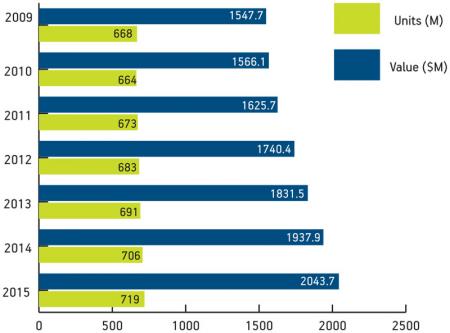
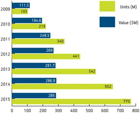
At the economic level, there are some MEMS sectors that are already very mature (e.g., inkjet print-heads (Figure 1), accelerometers for automotive airbag systems) and some that are in a phase of rapid growth (e.g., digital compasses (Figure 2,
p. 44)). Then there are others with great potential but which are still at the R&D stage.
Figure 1
Inkjet print-head market by volume and units, 2009-15
Figure 2
Digital compass market by volume and units, 2009-15
At the technological level, MEMS is inherently at the intersection of several engineering disciplines. In addition to electronic engineering, it has historically been closely associated with mechanical engineering. Beyond that, MEMS devices are frequently designed for real-world sensor applications requiring reference to fields such as materials science (especially for packaging) and environmental engineering. More recently, the advent of concepts such as the lab-on-a-chip has brought the technology into increasing contact with the world of biology. MEMS is arguably the poster child for the trend toward multi-disciplinary systems.
In short, the debate is not really about whether MEMS is happening or not, but rather whether certain applications within the space are happening and thereby have the scale to secure not just their own commercial viability but also, perhaps, help develop portable manufacturing processes that other applications can exploit.
Sources
This article is primarily based on two sessions at Semicon West 2010, held this year at San Francisco’s Moscone Center, July 13-15.
Jean-Christophe Eloy, founder and CEO of analyst firm Yole Développement (www.yole.fr), delivered the overview address “Status of the MEMS industry: emerging applications are (again) fueling the growth of MEMS markets.”
A panel session, “Optimizing manufacturing for future MEMS growth,” addressed production issues directly. Chaired by Karen Lightman, managing director of the MEMS Industry Group (MIG – www.memsindustrygroup.org), its four members were:
- Asif Chowdhury, a director in the Worldwide Manufacturing Organization at Analog Devices (ADI–www.analog.com);
- John Foster, CEO of Innovative Micro Technology (IMT–www.imtmems.com), a MEMS foundry based in Santa Barbara, California;
- Yan Loke, vice president of Engineering at Micralyne (www.micralyne.com), a MEMS foundry based in Edmonton, Canada; and
- John McKillop, managing director of the MEMS research company Tekton Consulting (www.tektonllc.com).
Market overview
As was the case throughout the electronics industry, 2009 was a difficult year for MEMS, according to Jean-Christophe Eloy. The few companies that grew tended to do so because of:
- acquisitions (e.g., Avago Technologies purchase of the bulk acoustic wave RF filter business owned by Infineon Technologies); or
- their involvement with emerging technologies that were growing from a comparatively low base (e.g., microphones, micro-barometers); or
- ongoing exploitation of markets that were mature in volume and therefore favored big players during the recession (e.g., Lexmark in print-heads).
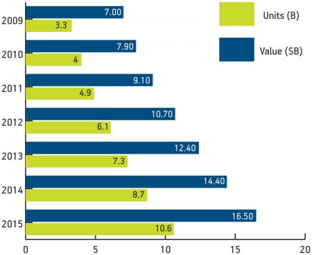
Yole estimates the 2009 value of the MEMS market was just under $7B, with a 13% return to growth set for 2010, followed by annual growth in the 2011-2015 period at a rate of 14-15%. This will bring the market to a value of $16B by 2015 (Figure 3, p. 45).
Figure 3
MEMS market by volume and units, 2009-15
“However, if you look at [the market] in terms of devices, the growth there is much more important. It will go from close to 3.2B units in 2009 to more than 10B units in 2015,” added Eloy.
He cited the cost-down demands of the consumer electronics and automotive industries as exerting the greatest pressure to reduce prices while ramping volume by more than 3X. Moreover, he expects rapid growth in demand for some newer products, led by digital compasses that are being integrated into cellular handsets to provide location-based services. These compasses alone are expected to represent 2.2B of the devices sold in 2015, just a little below 14% of the overall space.
Eloy noted that manufacturing has a critical role to play in enabling the market’s development as MEMS also moves from a functional model to a system model that places greater emphasis on elements such as software.
“We used four- and six-inch wafers in 2000 and now we are moving to six- and mainly eight-inch wafers by volume,” he said. “Only a few players might be on eight-inch, but that is where the majority of growth is happening based on manufacturing capabilities.
“We have also moved from wire-bonding side-by-side to stacked die. There is more innovative packaging and companies are using it for added value. We have then also moved to SOI [silicon-on-insulator] wafers and epi-poly approaches to silicon. And we have removed capping and implemented 3D TSV [through-silicon-via].
“All of these things are already in development or in early production.”
Another major contributor to the battle over manufacturing costs is the growth of the foundry sector. It has long been the natural home for start-ups delivering products in low-to-medium volume, but today many major MEMS producers are also outsourcing production rather than operating their own fabs.
During the panel session, ADI’s Chowdhury said that his company is looking for more third-party providers. In his presentation, Eloy noted that two major players in the automotive space, Delphi and Continental Automotive Systems, had recently stopped in-house manufacturing and switched to foundries, and more were likely to follow.
“It’s been a key trend over three years and has been amplified by the downturn in the last year,” Eloy said. “According to the data we have, at least five companies are involved in such changes at the moment with a total business value of $350M. That’s a huge transfer to the foundries.”
This is not entirely new—STMicroelectronics (ST) has long provided foundry services for Hewlett-Packard (HP), for example—but it still represents a massive vote of confidence in third-party manufacturing.
However, Eloy also cautioned that economies from reuse might still be constrained, even though this has been fundamental to the foundry model in mainstream semiconductors. He said that the simplification of manufacturing is still more an objective than a reality for most MEMS.
“The ‘MEMS flow’—one product, one process, one package—is still there,” he said. “I first identified this issue in 2001 and it still has not been solved for most companies.”
ADI’s Chowdhury noted that such fragmentation could be seen across the same organization. “It can be the case that even within one company, there is no standard. There are different test platforms, different packaging platforms,” he said.
This kind of dispersed effort may be costing the MEMS industry dearly. Yole’s research shows that it takes an average of four years to bring a product to market at a cost of $45M, with a company burning through three or four CEOs in that time. Such figures might seem modest in comparison with the NREs dogging chip design at advanced nodes, but it again needs to be remembered that many MEMS devices today typically target small, almost niche markets. Eloy said that only a handful reached into markets with a value of more than $200M.
Manufacturing challenges
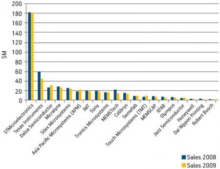
The foundry market is growing. Yole ranks the top 20 suppliers, of which six now have sales in excess of $20M annually (Figure 4). This is obviously some way behind the chip foundries, but with more business being transferred into the sector all the time, confidence is high.
Figure 4
Top 20 MEMS foundries
Nevertheless, the two foundries represented on Semicon’s manufacturing panel acknowledged that there are major challenges ahead, the first of which is ending the dominance of bespoke processes.
MEMS innovators often do not understand the economic roadblock this represents. As Micralyne’s Yan Loke noted, “You can come to us with a process that you’ve developed at, say, university and that was manufacturable in that environment. But don’t come to us and simply assume you can say, ‘I’ve made one of these, now can you make millions?’
“The customer has to understand that making a million is very different from making one. There’s a learning curve; there’s going from prototype to production and that takes time and money.”
There are some big companies involved in the MEMS space. Many of the companies mentioned in this article count among technology’s 800 lb. gorillas. Across this band, there is plenty of influential R&D work underway. ST, for example, is promoting a new generation of accelerometer, gyroscope, microphone and compass products.
However, most innovation in MEMS comes from start-ups. Cost control in such companies is always important, even more so at a time when investment capital is as constrained as it is today. This puts foundries high up the agenda. IMT’s John Foster noted, “You’re not Hewlett-Packard. You’re not Analog Devices. You can’t afford to go out and build your own fab.”
In that context, Tekton’s John McKillop stressed that, “The thing I keep telling my clients is that the choice of foundry is the most significant decision a start-up is ever going to make. It’s their most significant financial decision and it will have more to do with their success or failure than any other one they take. They have to be careful. They have to be methodical. And they have to execute.”
Basics
MIG’s Karen Lightman said that her association is in the process of creating a foundry checklist that companies can use to guide their choices, but in the meantime, the panelists did say that there were some obvious guidelines. The first of these was to exploit reuse.
“The way to be successful and really help the customers is to come up with more platforms that are reproducible and reusable,” said IMT’s Foster. “That’s really what people need. It speeds up development, and lowers the cost enormously.”
His company is using its involvement in numerous technological areas to facilitate as much of a shift away from the ‘one-process’ constraint as possible.
“We’re in all these different businesses, so we can survive, we have the economic diversity,” explained Foster. “And there’s something that happens when you get the economic diversity and that is that you get a technical diversity from working with customers in all these different areas.
“So, we might make a breakthrough in a biomedical application and turn that around and use it in a high-end navigation application. That happens literally every week—and it’s very exciting.”
The implications here for the customer are strong and implicit, and Loke spelled them out. “If you want us to develop a process for you, and you have buckets of cash, then we’ll do it to suit your requirements,” he said. “But if you’re a start-up, it’s always good to fit in.”
‘Fitting in’ goes beyond simply assessing the process modules and turnaround times that the various foundries have and then deciding which are best for your project.
“It’s not just about finding capacity,” said McKillop. “It’s about finding a fit at the management level, at the expectation level, at the IP [intellectual property] level, at the whole range of levels in the company and then executing.”
Standards
There is another side to the alignment-reuse debate and that is the obvious concern that some companies will have about developing a product that is so closely tied to one manufacturer’s processes that they are effectively locked in.
Chowdhury noted that even a company of ADI’s size faces a challenge when it wants not simply to outsource, but to have multiple foundry partners—already necessary in its case, where much of its parts roster is subject to the seasonal peaks and troughs in demand that come from end-use in consumer electronics.
More standards for fundamental process steps would help here, although there is some debate as to whether the multi-disciplinary nature of MEMS makes this an insurmountable challenge.
“One moment you’re working with optical MEMS. Or then it’s accelerometers. Or gyros. And we do a lot of things related to biology,” said Foster. “It’s not that standardization isn’t a good idea. There are just so many things, it’s impossible.”
However, there are those who say that within the technological panoply, there are some issues that could be addressed specifically. Again, Chowdhury noted that companies bringing their own internal operations into line could be an important starting point.
“Maybe as a first step, companies could come up with one advanced packaging platform to serve all their needs,” he said. “That in itself would be a huge move in serving the need to reduce costs.”
McKillop, however, suggested going substantially further. “This is one of my favorite soap boxes,” he said.
“I think that the critical issue our industry faces will be the availability of an open-source process at a large foundry. It doesn’t have to be a well-defined PDK or have all the fancy design tools that you have for CMOS. But it’s got to be open-source, so it’s available to all comers with clear design rules in a high-volume, low-cost fab. I think that the evolution of that kind of process will make us a well-defined industry in the future.”
McKillop has a point. As stated above, the current Yole numbers show only six foundries with annual sales of more than $20M, and yet growth in the MEMS market is being driven by consumer electronics where demand can move up or down by millions of units over the course of a quarter. Portability and consolidation would appear inevitable over the medium term, and therefore broader standardization will be necessary. The willingness—and desire—among volume customers to adopt third-party manufacturing should also drive this trend.
In the meantime, exploiting such reuse as is available and following the general design-for-manufacturing maxim of pushing process considerations (as well as those for packaging and other back-end elements) to as early as possible in a design flow would appear both logical and necessary in the short term.
Progress is taking place, but it is vital that it continues because system design is becoming more pervasive. “The evolutionary steps for MEMS manufacturing have been surface micromachining in the 1980s, bulk micromachining in the 1990s, then the thick SOI, then thin SOI, cavity SOI, and now CMOS-MEMS integration, not just side-by-side but chip-to-chip, one on top of the other,” said Eloy.
Beyond this, MEMS manufacturers also need to free up resources, as is happening in mainstream semiconductors, to spend more time providing the software and other elements that lead them to market.


