Mounting Fiji: How AMD realized the first volume interposer
AMD’s Radeon R9 family is the result of eight years developing 3D-IC and interposer technology. What lessons did the company learn?
In June, AMD launched its Radeon R9 graphics cards. It is the company’s first family to feature die-stacking and its proprietary High-Bandwidth Memory (HBM). AMD further claims these are the first ‘volume’ interposer products.
There have been two overarching commercial goals. The first and most obvious was to introduce AMD’s latest generation GPU – previously codenamed ‘Fiji’ – for the 4k and VR gaming markets. The second was (and is) to create and mature an interposer/stacking technology platform that AMD can extend across all its products.
The flagship of the range so far, the Fury X, stacks the GPU on top of four HBM die. The GPU has 1050Mhz clockspeed with 4096 SPs organized into 64 CUs. The memories, thanks to the TSV construction, have a fat 4096-bit memory bus clocked at 1Gbps (500MHz DDR). This makes for 512GB/sec of memory bandwidth, fed by 4GB of HBM organized in stacks of 1GB each. It’s a 60% increase in memory bandwidth achieved without the kind of power penalty that has been dogging GPU configurations
The gaming performance of the cards – so far, the Fury and Nano have also been launched – has been widely discussed on gaming and benchmarking sites. Less has been said about Fiji’s overall development process and what lessons it might hold for others planning for 3D-IC.
During the SiP Global Summit earlier this month at Semicon Taiwan, AMD Fellow Bryan Black, one of the project’s leads, shared some war stories – or more accurately pointed to one interconnected story that he sees as representing the greatest challenge presented by 3D-IC.
Motivation for 3D-IC
Dr Black referred to a graph that has appeared in similar variations within the GPU community over the last few years to remind his audience why AMD has moved to interposer-based boards. The shift has long been planned.
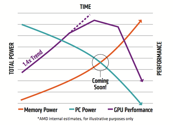
Figure 1. GDDR5 can’t keep up with GPU performance growth (Source: AMD)
Figure 1 shows three lines. In purple, it depicts the GPU flavor of Moore’s Law which envisages roughly a 40% performance increase every year. The orange line represents memory system power, and how it would be likely to increase based on a traditional graphics board architecture. The blue line shows what is left after meeting memory’s demands for computation.
“You can see that over time we’re running into trouble,” Dr Black explained. “We starting with an interesting distribution where the vast majority of power is allocated to compute. But over time you see the compute allocation going down very fast and the memory allocation going up very fast. Before you know it, you have a system where you can no longer improve performance.”
He added that having identified this problem “about seven or eight years ago”, AMD decided to put memory integration with GPU at the forefront of its existing research effort into die-stacking and other aspects of 3D-IC. This was the technology that would head off that power crunch.
The company ultimately achieved that by exploiting the key features of 3D-IC. “We took the technologies that you’ve heard about so many times – the microbump interface, the very narrow pitches – and we went to an extremely wide DRAM interface [4,096 bit], slowed down the interface to 500MHz , and then we could simplify everything,” explained Dr Black.
“By doing that, we went from that kind of non-linear power growth to a very linear power regime. Very simple structures consume very little power, and what they do consume they take extremely efficiency. So, we were able to get 60% higher bandwidth and 60% lower power than our product from the year before.
“In terms of gigabyte of bandwidth per watt, it’s a 4X improvement over the previous generation of GDDR5. That’s massive. And it’s not just the DRAM. The interfaces on the GPU also consume much less power.”
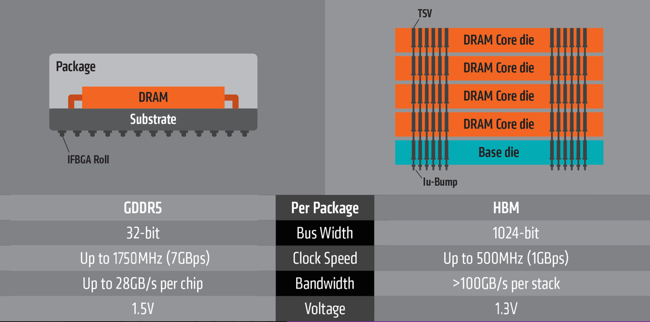
Figure 2. GDDR5 compared against interposer-based HBM (Source: AMD)
So, job done. But, Dr Black’s main argument was that it took a lot of work, investment and risk to get there.
Interposer prototyping for feasibility
“We predicted that the problem would hit in the 2015-16 timeframe and that we had to do something new,” said Dr Black.
That something new emerged after a number of 3D-IC prototyping and delivery stages. These were divided into:
- 2007-11: Concept, first steps.
- 2011-2014: Primary learning to feasibility and supply chain definition
- 2014-2015: Final product development, bring-up and delivery
AMD undertook numerous prototypes within each of these stages. Dr Black estimates around 15 in total.
For example, during the initial phase, AMD concentrated on a vehicle that placed GDDR3 memory next to a Griffin (Turion X2 Ultra) generation CPU in a mechanical stack. R&D at this point was conducted internally and chiefly with Germany’s Fraunhofer Institute.
“[This early work] taught us the real challenges and not just the technical ones like warpage, but the real challenges in how you acquire the silicon, glue it all together and then test it,” said Dr Black.
As this work progressed, AMD added more partners. Still in the first phase – around 2009 – the company began working with SK Hynix on what would become HBM: the existing ATi RV635 GPU was combined with a custom DDR3 die-stack with TSVs.
Over time, OSAT, foundry, packaging and more partners were added, features were shrunk, further reliability and test vehicles were added. But it was not until 2012 that the team had a prototype structure that “convinced us we could build this thing and should spend serious money”.
More refinement and productization followed as work entered the critical third phase. “Toward mid-2014, we realized that the GPU was going to be quite large, so we started moving to larger devices. Specifically all the functional devices needed to be hooked up to a 500 sq mm ASIC in the prototype,” Dr Black explained.
“We didn’t have a 500 sq mm ASIC at the time, but we did have one where if you chopped out four of them at a time, they would match a 500 sq mm ASIC. So that’s what we did, then we powered all four die – some of them fully functional – and moved forward. The functional aspect was important there for our electrical test requirements.”
This was followed by the ‘Fiji Replica’, a 600 sq mm ASIC sitting on a 1,000 sq mm, with essentially the same dimensions as the final product.
“We realized this was quite expensive, so we went through a tremendous cost-down effort, eliminating complexity, anything we could get rid of,” said Dr Black. “I think we were able to reduce about 50% of the cost. That gave us a shippable solution.”
As its efforts neared fruition, AMD concluded that the main challenges in the development process had proved to be significantly different from those it had expected.
“When we started the program we thought it was all going to be about developing TSVs, developing microbumps and figuring out how to attach die,” Dr Black told the SiP Forum. “What we quickly learned is that it was actually about developing a supply chain, creating new technology partners and changing the roles of the companies we worked with.
“Our foundries started doing different things. Our OSATs started doing different things. Our DRAM vendors were taking on much different activities. Even our approach to how we’d test a part. All these things changed.”
The combination of skills required to realize an advanced interposer product introduced an inevitable domino effect: change one thing and many more were altered. Both in the prototypes and in the finished product, AMD concluded that with a complex and shifting supply chain in place, “If we came up against a business or technical challenge, we went back and changed the design to get rid of it.”
Record breaking bring-up
“I don’t think any one challenge was hard. It was their interaction,” reiterated Dr Black.
Yet when AMD looked to apply its interposer learning in anger, things went remarkably smoothly.
“The program’s key accomplishments are that 12 hours from having our first sample in hand, we were booting Windows and we were running games,” said Dr Black.
“Within five days we had completed our entire bring-up of the product and could shut those activities down. Usually they had taken three months. And we were shipping within six months of the first ASIC wafer.
“This was the fast bring-up and execution of a program ever at AMD. Development of the first R9 cards began in mid-2014 and they were going out the door by this June.”
But it was only possible because of the eight years of work before hand. And thereby hangs a tale.
AMD is unquestionably a Tier One player, the kind of company expected to take a lead in the implementation of new technologies. But it is still significant that as it moved through a lengthy 3D-IC development process, it was essentially making it up (or figuring it out, if you prefer) as it went along.
Conclusion
A recurring theme in the SiP world is the current lack of standards. Given that the technology involved remains difficult – though not, as AMD’s work shows, insurmountable – users essentially have to develop their own flows and infrastructure.
It is unlikely today that a company would need to spend seven or eight years doing that, but there is still a lot to mix and match. As the Radeon R9 shows, change one thing and the results cascade through the project.
The upside, of course, is that AMD’s ambitions have drawn suppliers along with it. UMC’s TSV technology can now be considered somewhat battle-hardened. SK Hynix has further demonstrated its capabilities in stacked memory.
There is know-how in place. Nevertheless, the main message from AMD’s experience stands: it is still likely to take some effort and skill to knit all that together.
