IP-to-SoC prototyping demands consistency
Porting your IP to the FPGA-based prototype of an SoC design is hazardous. Particularly for new blocks, the process often involves some form of translation that can introduce errors. Sometimes, the system design team finds itself repeating verification already undertaken by the IP’s developers. These are just two of the more common concerns.
Overall, engineers need an infrastructure that reduces risk, reflects shrinking project deadlines and brings greater consistency to the IP-to-SoC flow. Let’s look at why you should and how you can achieve that.
The risks of mix-and-match
It is often the case that the IP-to-SoC FPGA-based prototyping process will involve different tools and different boards across the two stages. Bridging this divide is where many of the problems arise. They can be illustrated by looking at the main obstacles presented in terms of how the IP is delivered to the SoC team. Typically, this is done in one of three ways:
- As RTL
- Encapsulated as a ‘physical’ hardware deliverable
- As both an IP block and an FPGA binary
1. RTL deliverables
The RTL option has the benefits that it represents a portable ‘soft’ delivery and provides such flexibility that the code can be tailored to fit any SoC platform.
But SoC teams will often find themselves duplicating much of the earlier IP prototyping and verification effort.
If the platform and tools on which the IP was developed differ from those being used by the SoC team, there is a greater likelihood of model mismatches. This mismatch issue is obviously a concern where working with third-party IP suppliers.
However, a further issue arises for third-party partners: the lack of sufficient protection for the IP. Externally and internally, some encryption is desirable.
2. Physical hardware deliverables
A physical board offers the advantages of validated delivery in a format that should have been tuned to the configuration of the prototype. So, it should only involve a single prototyping effort, shouldn’t it?
Well, it might, but it is also expensive: there are now two prototyping boards where only one was probably necessary. However, this may be the design team’s preferred way of working. Still, there are other factors to consider.
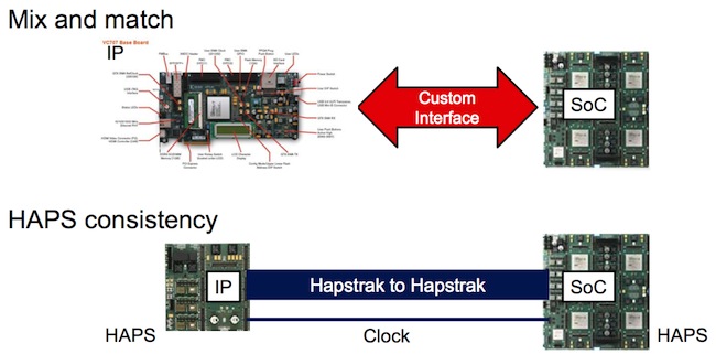
In our inconsistent mix-and-match world, connecting the IP board to the SoC board typically entails extra work creating adapters and custom interfaces, both of which then need their own debug. There is also no guarantee of clock synchronization.
3. FPGA binaries
An FPGA binary looks like an all-round winner. It’s validated, it’s tuned and it involves a single prototyping effort.
But you can only feed forward these binaries where you are using the same FPGA platform at both the IP and SoC prototyping stages. Any mix-and-match of in-house and third-party boards makes it effectively impossible to do.
Consistency with HAPS-70
The obvious answer is to align your IP and SoC prototyping environments as closely as possible.
We’ve discussed juggling the use of different types of board and design software at the stages in your IP-to-SoC prototyping flow. Beyond that though, it’s fair to ask how many of the tools needed to realize both the IP and the SoC the prototyping board vendor provides. Often, the beyond-silicon support is limited and the gaps are significant.
Synopsys has developed an integrated flow based around existing tools and its Xilinx Virtex-7 2000T-based family of HAPS-70 boards, embracing both the hardware and the software needed to provide consistency. You can thereby minimize risk and reduce prototyping time.
Let’s look again at the three IP delivery models but in the context of HAPS-70.
1. HAPS-70 and RTL deliverables
IP can be developed and prepared for FPGA-based prototyping utilizing Synopsys’ Certify and Synplify Premier software tools. These tools are applicable to usage at both the individual IP level and higher SoC level. This enables direct script reuse, saves time and increases confidence in the block being fed through.
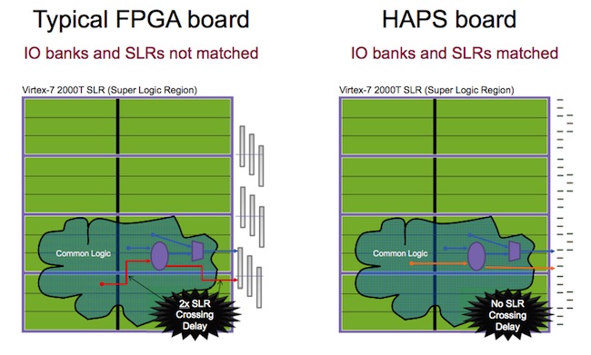
The target hardware is also consistent at both stages. HAPS-70 has a modular and symmetrical system architecture to smooth the transfer from, say, a single to a multi-FPGA-based system. Moving daughter boards and related connection pin-outs has a minimal effect on timing and performance as the HAPS-70 I/O connector banks directly map to the super logic regions (SLRs) found on the 2000T. The 1:1 SLR-to-bank-to-HapsTrak connector ensures uniform timing characteristics.
Figure 1 Failing to map directly to SLRs can lead to crossing delays
2. HAPS-70 and physical deliverables
Simply put, you’re now working withing the same IP-to-SoC flow, the same environment. There’s a single IP FPGA bit image file for both the IP and SoC stages. Connection between the two systems is over the common HapsTrak interface. Translation and debug risks are thus mitigated. Clocks and resets are synchronized by the inbuilt HAPS-70 capabilities.
The system allows for high-speed time-domain multiplexing between systems to raise FPGA-based prototype performance. Configuration over UMRBus is quick and easy. And the IP can now be locked and encrypted.
Figure 2 Common interfaces reduce risks in developing custom alternatives and synchronize timing
3. HAPS-70 and FPGA binaries
Here again, the use of the same consistent platform overcomes the otherwise near insuperable obstacle facing this IP-to-SoC prototyping model.
In addition to your ability to feed through the same FPGA bit file of your IP, there are the further benefits that both daughter board placement and the connectors are identical.
What we all really need
By the time that a typical SoC project has reached FPGA-based prototyping, the design team wants to focus on issues that could affect the user experience in the target design. Do the various IP blocks in the design function as intended and fit together in the whole? What happens when you expose them to real-world inputs and multi-processor software?
If the prototyping infrastructure itself introduces delays and irrelevant bugs, the technique’s advantages are greatly diminished. The rational answer then is to adopt an IP-to-SoC infrastructure that offers most consistency from initial IP development through to final silicon.
HAPS-70 has been configured to do just that. With IP and SoC teams working in the same environment, communication between them will improve. And your engineers can focus on the needs of the final silicon as quickly and as efficiently as possible.


