Interoperable PDKs accelerate analog EDA innovation
Process design kit (PDK) standards are one area that could greatly help reduce the disproportionate time and effort required to realize the analog portion of a design. PDKs have existed for two decades and provide access to foundry-verified data files for such AMS design elements as parameterized layout cells (PCells). However, most have been constructed using proprietary languages and databases, and this works against easy reuse, multi-vendor tool flows and other potential efficiencies.
As advanced process nodes require access to complex PCells, complex design flows and IP portability, open standardized PDKs are becoming a necessity so that analog designers can take full advantage of the latest technologies. April 2007 saw the establishment of the Interoperable PDK Libraries (IPL) Alliance, an industry-wide initiative charged with establishing an interoperable custom design ecosystem.
Some 18 EDA vendors and Taiwan Semiconductor Manufacturing Co. (TSMC), the largest foundry, are now members of the alliance, and the article describes its work to date, including an already-demonstrated multi-vendor analog design flow that uses the new standards.
While digital design automation has progressed with amazing speed over the last 20 years, analog automation has lagged far behind. With RF and consumer devices demanding increased integration, the analog portion is now the gating factor for many, if not all system-on-chip (SoC) designs. This disparity exists because analog is fundamentally harder to automate than digital. During the planning stage of a SoC design, managers use the following rule of thumb for scheduling the analog content: 2% of transistors = 40% of design effort.
Much of the analog portion requires painstaking manual effort that consumes nearly half of the overall design team effort. However, while customers have the economic motivation to automate analog design, limited tools are available. The problem is further compounded by the high effort required to evaluate and then adopt analog automation tools.
This scarcity is not just a technology problem that has resulted from a lack of innovation. Even if engineers could get the tools, they would still lack the infrastructure required to support a viable ecosystem. Such an ecosystem would need several companies working together to fill every niche and competing to provide the best solution. However, before you can have a vibrant eco-system, you need a set of standards that enable interoperability. Process design kit (PDK) standards are one area that can provide substantial benefits to the custom design ecosystem.
Source: Synopsys
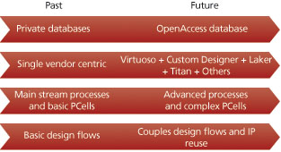
FIGURE 1 PDK trends
A PDK is a comprehensive set of foundry-verified data files including parameterized layout cells (PCells) that are used in an analog and mixed-signal design flow. There has been little to no innovation in PDK technology for the past 20 years. Traditionally, PDKs were written in proprietary languages and operated on proprietary databases. Proprietary SKILL-based PDKs have limited design reuse and prevent designers from adopting best-in-class tools. With the adoption of the OpenAccess (OA) database by many large IDMs and semiconductor companies, more and more EDA vendors have introduced modern automation tools that support the OA standard to address analog design challenges. Nowadays, more designs are moving to advanced process nodes that require complex PCells, complex design flows and IP portability (Figure 1). However, if analog designers are to take full advantage of the newer EDA tools, advanced process technology and design flows, they must have open interoperable and standardized PDKs.
Common standards
In April 2007, four EDA companies—Applied Wave Research (AWR), Ciranova, SpringSoft and Synopsys—started the Interoperable PDK Libraries (IPL) Alliance. It is an industry-wide initiative charged with establishing an interoperable custom design ecosystem. Some 18 EDA vendors and Taiwan Semiconductor Manufacturing Co. (TSMC), the largest foundry, are now members.
The alliance’s current focus is on interoperable PDKs. Members collaborate on the creation and promotion of interoperable PDK standards that work with any OA database tools. Since its inception, the IPL Alliance has released a proof-of-concept interoperable PCell library, demonstrating interoperability among tools from multiple vendors. In October 2007, IPL announced the formation of three technical working groups to advance this work in areas of particularly importance: PCells, Properties and Parameters, and Constraints. These three fields have been identified as having the potential to gain the most benefits when standards are applied. With this announcement, the IPL Alliance expanded its charter to address broader interoperability issues with foundry PDKs and design flows.
TSMC specifically joined the alliance at the 2008 Design Automation Conference (DAC), and began working with key IPL Alliance members on a TSMC 65nm interoperable PDK. At DAC 2009, TSMC announced the availability of the industry’s first interoperable PDK (iPDK). The TSMC 65nm iPDK is supported by all major EDA vendors including Cadence Design Systems, Ciranova, Magma Design Automation, Mentor Graphics, SpringSoft and Synopsys. For the first time in semiconductor industry history, IC designers will be able to use the same PDKs in tools from multiple vendors and tools they have developed in-house.
An interoperable PDK benefits the entire chain of semiconductor companies, foundries and EDA vendors. Semiconductor companies can use one unified interoperable PDK to provide advanced functionality across multiple EDA vendor tools, improve design accuracy, shorten design cycle times, and promote design reuse and IP portability. These benefits improve the return on design investment. Foundries can reduce their PDK development, validation, support and distribution costs while expanding the number of tools they support. EDA vendors will also be able to reduce PDK development costs while supporting a wider range of foundry partners.
Without interoperable PDKs, each foundry has to create multiple tool-specific PDKs for different EDA tools. The numbers are staggering. TSMC alone developed, distributed and maintained 2,500 PDKs and technology files in 2007. The standardization of PDKs benefits analog and custom IC designers by removing bottlenecks in multiple-vendor flows. Standardization can reduce PDK development cost and schedule, providing designers quicker access to new, advanced process technologies.
Key PDK features
The iPDKs (Figure 2) are based on the OA standard and use standard languages such as Tcl and Python to ensure interoperability among all EDA vendor tools. These iPDKs include a comprehensive set of APIs to enable customization, support advanced PDK features and provide an interactive environment for PDK development. PCells written in Python (PyCells) not only have significantly fewer lines of codes, but also provide tremendous performance improvement compared to relative object-based (ROD) SKILL PCells. PyCells support advanced features such as abutment, stretch handles and DFM rules. PyCell Studio from Ciranova provides an interactive development environment (IDE) for PyCell development and efficient PyCell debugging, therefore improving PCell development productivity and shortening the PDK development cycle.
Source: Synopsys
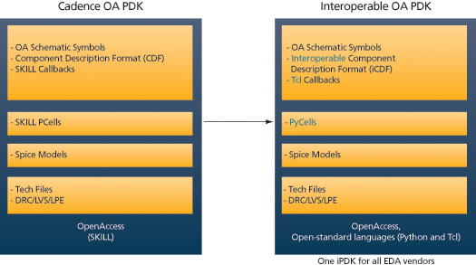
FIGURE 2 Proprietary OA PDK vs. interoperable OA PDK
Development efficiencies result in faster PDK delivery to users and allow more resources to be applied to create more device types and more device features. High-level Python APIs provide process porting capability within PDKs. There is no need to code PyCells for different processes because designers can just swap out tech files. This has great benefits for IP groups. Interoperable PDKs have all the features supported by SKILL-based OA PDKs and more. Analog designers not only get to use a single PDK for all EDA vendors’ tools, but also a better, faster PDK with more features and capabilities. Because interoperable PDKs are based on OpenAccess and only use open-standard languages, no stream-in or stream-out or any form of data translation is needed among the leading physical verification tools. This makes PDK validation easier and more efficient.
Multi-vendor flow
The progress of the IPL Alliance’s efforts was showcased at DAC 2009 in a jointly developed TSMC 65nm iPDK prototype used in a multi-vendor flow (Figure 3). This example illustrated how designers can take advantage of iPDKs and choose the best-in-class tools for their design flow.
A low noise amplifier (LNA) circuit was created in Synopsys’ Galaxy Custom Designer environment using standard OA schematic symbols and saved in the OA database. The schematic was opened in SpringSoft’s Laker to view the same exact circuit. The LNA circuit was then simulated using Synopsys’ HSPICE simulator. A schematic-driven layout of the circuit was created using Laker, saved in OA and re-opened by Synopsys’ Custom Designer, where some PCell parameters were changed to create intentional design rule check (DRC) violations. Mentor Graphics’ Calibre was then used for running DRC to show violations; the Laker layout was used again to fix the DRC violations. Synopsys’ Hercules physical verification then opened the layout and ran clean DRC and layout vs. schematic (LVS) comparisons. Synopsys’ Star-RCXT parasitic extraction was used to run extraction and back annotation to demonstrate the post layout flow.
During the complete analog front-to-back multi-vendor flow demonstration, only one TSMC 65nm iPDK was used. The design data was stored in OA and was directly read, modified and written by all tools with no translation at any point. The interoperable PCells were built using Ciranova’s PyCell Studio tool based on the open source language Python. This was a major achievement for the IPL Alliance.
Source: Synopsys
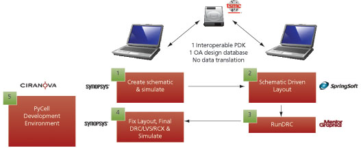
FIGURE 3 Complete multi-vendor front-to-back analog flow
For the first time in analog EDA industry, customers can take advantage of best-in-class tools from their choice of vendors.
Analog design has been characterized as ‘black magic’ because of its comparative difficulty and complexity. Much of the work is still done with less automation compared to digital design. Using iPDK standards as the building block for analog design will enable design reuse, improve design productivity and ultimately promote innovation in analog and full custom EDA.
Synopsys
700 East Middlefield Rd
Building C
Mountain View
CA 94043
T: +1 650 584 5000
