Innovations at ITC 2010
Poster sessions are all too often given Cinderella status at major conferences, but they often contain novel and interesting responses to current technology challenges. This article reviews five poster papers that were released at the 2010 International Test Conference ranging in topic from improved device interfaces for gigahertz test to IP security to the diagnosing of increasingly prevalent open defects. Sources for the work include Bell Labs, BITS Pilani of India, Freescale Semiconductor, Mentor Graphics, Texas Instruments, France’s University of Montpelier and CNRS research group, and the University of Windsor.
MEMS device interface board
A traditional device interface board (DIB) degrades significantly at the very high frequencies that need to be used to fully test today’s devices, but what about a DIB based on emerging microelectromechanical systems (MEMS) technology? Such a proposal was published at ITC by scientists from the University of Windsor in Canada.
In a traditional DIB configuration, the signal path from the pins in automatic test equipment (ATE) hardware to a device-under-test (DUT) can suffer from discontinuities, long wire traces, parasitic capacitance and inductance. In the gigahertz range, these systems pick up considerable noise and exhibit high distortion. The effects on transmission lines become critical and require matching impedances to minimize signal reflection.
Also, AC resistance due to the skin effect and electromagnetic coupling caused by radiation harm signal integrity and reduce accuracy.
“In the design of a DIB, the greater the physical separation of the DUT and the ATE pogo pins, the greater the distortion and signal degradation,” the Windsor team notes. “A MEMS-based DIB can lower the distance between the DUT and the ATE pogo pins by orders of magnitude due to its micro-scale dimensions.
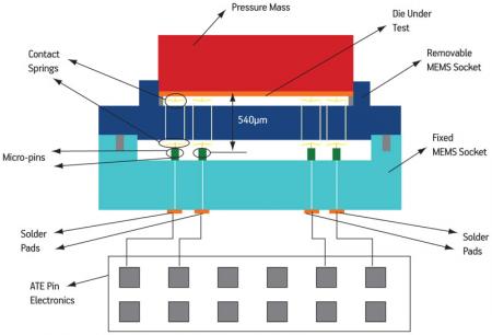
The researchers are evaluating such a DIB that features both a fixed and a removable MEMS socket (Figure 1).
Figure 1
Proposed MEMS-based device interface board
“The fixed socket contains solder pads designed to be connected directly to the ATE pin electronics. It also includes a bed of micro-pins used to establish electrical connections between the removable socket and the ATE pin electronics. These micro-pins are in fact the substitutes for conventional pogo pins,” they report.
“The removable socket incorporates contact springs providing temporary connectivity between the DUT pads and the ATE resources. Test interface circuits, if required, can also be mounted at the die level on the removable socket.”
Work to date has already covered electromechanical simulations, which point to low resistance paths between the DUT and the ATE resources, with DC resistance below 100 mΩ.
Electromagnetic simulations and SPICE models for the contact springs suggest that the proposed DIB scheme can operate up to 50GHz without much loss or distortion (10 fF capacitance, 200pH inductance, and 0.3Ω resistance). That metric is important because traditional DIB configurations would, at that operational level, begin to suffer badly from AC resistance in the paths and parasitic capacitances and inductances.
“The MEMS-based DIB reduces the undesired effect of transmission lines considerably. It will also lower the cost of fabrication by providing necessary means to detect faults at the die level before packaging,” Windsor’s researchers write.
The work is contained in the paper “A MEMS-based device interface board”, Poster #4 from the 2010 International Test Conference.
Securing the scan chain
JTAG has become essential to the development of effective design-for-test strategies and also for embedded systems debug, maintenance and recovery. However, the access provided for necessary tasks can also be used to hack into and reverse engineer a system or extract secure data.
One option involves removing the JTAG test access port (TAP) after factory testing. A problem here, though, is that the confidential data may remain on the board and could be accessed using probes. Secure storage and fuses can provide greater protection but these can often add too much overhead.
A team from Alcatel-Lucent Bell Labs in the US and Bell Labs in Dublin, Ireland has now proposed a scalable technique for securitizing scan chains using a new JTAG primitive.
It calls the approach an Open-Circuit Deadlock (OCD). It is a one-bit scan register with almost no cost or overhead, and its form (Figure 2, p. 52) resembles the segment insertion bit cell that forms part of the proposed IEEE standard, P1687. It differs in three significant ways.
Figure 2
Open-circuit deadlock
- The derivation is left as an open circuit.
- The cell OCD/UpOCD is after the derivation.
- The UpOCD cell is reset by the port ‘SecureRST’ and not, as is usual, by the scan chain reset.
As a result, the scan chain is broken once OCD is asserted—it is deadlocked with regard to normal access. However, SecureRST can be asserted to unlock the chain. The complexity of the security now varies according to how that process is configured and achieved.
The Bell Labs group offered four models:
Secret key unlock
A key is scanned into one of several chosen locations (e.g., the interrupted chain or a separate one) to generate the SecureRST signal. The key itself can be as simple or as complex as is felt necessary. A challenge-based format can be used.
Cascaded interlocked and remote OCD
Because an OCD is only a one-bit register, the user can replicate many of them in a single scan chain and require them to be, say, unlocked via different SecureRST signals in a particular order.
“Similarly, the control bits and the open circuit do not need to be contiguous: as long as the deadlock condition persists they can be placed in different positions on the scan chains (or on different chains), to obfuscate the architecture and make reverse-engineering more difficult,” the team also notes.
TAP locking and special sequences
An OCD can be located inside and, when necessary, lock the TAP instruction register. The instruction to unlock the register could need to be sent from a separate component on the chip (e.g., a processor), or require a special tap sequence (such sequences are already available in the IEEE 1149.7 standard).
Board and system level
The technology’s promoters say that where OCD and SecureRST signals are in the same chip, probing and tampering are impossible. Each chip will usually have its own custom securization scheme. However they add, “It is nevertheless possible to imagine board and system-level approaches, as long as the SecureRST signals are kept secure (for instance, by routing through hidden layers).”
The work is discussed in the paper “Scan chain securitization through open-circuit deadlocks”, Poster #8 at the 2010 International Test Conference.
Soft errors in memory
Researchers at two of France’s leading engineering schools—the LIRMM at the University of Montpelier and CNRS, also in Montpelier—have developed a modular, programmable, portable and low power consuming testbench to detect soft errors in memories.
Memories can occupy a huge portion of the surface of a system-on-chip, sometimes more than 80% of the real estate, and suffer the greatest probability of experiencing an error that leads to a malfunction of the entire device. Another particular concern is their susceptibility to the environment, so the testbench is geared to problems that may be induced by factors such as altitude, latitude and particles (neutrons, alphas, etc).
The team needed to consider trade-offs between elements such as power consumption, bit-flip coverage, modularity, programmable online test algorithms, remote system control and test data acquisition. These led it to opt for a built-on-board self-test (BOBST) architecture over traditional built-in self-test (BIST).
In BIST, each circuit carries embedded test circuitry; BOBST manages memory test at board level and can be configured to test multiple systems.
“Besides reducing the consumption (if compared to standard automated test equipment), this method offers the advantage of allowing the boarding of standard memories and by consequence the implementation and exploration of various technologies,” the Montpelier researchers report. Meanwhile, to keep power consumption low, all groups of memories are driven by a single scheduler.
BOBST works for memories in both static (hold) and dynamic (with read/write operation) modes, and these can be combined to detect soft errors in both sequential and combinational logic.
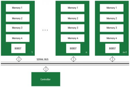
The testbench distributes the memories in independent subsystem modules composed of four memory chips connected to a single IC BOBST (Figure 3).
Figure 3
BOBST testbench architecture
Each subsystem, ‘n’, is connected to a central control unit through a serial bus. The choice of a serial bus was made to reduce power consumption and wiring. Another reason was the limited amount of data that circulates on the bus:
- subsystem module diagnostics information;
- enabling signals for switching subsystems off and on to lower power consumption and detected malfunctions;
- reprogrammed test algorithms (March type) operated by the IC BOBSTs; and
- test failure data.
The BOBST then undertakes these core actions:
- test pattern generation;
- test sink;
- storage of test failure data; and
- transmission of test data to a central control unit.
The work is described in Poster #10 from the 2010 International Test Conference.
Closing down opens
Although stuck-at and transition fault patterns can catch many interconnect opens, they cannot get them all and they remain one of the main sources of design failure.
Researchers at Freescale Semiconductor and Mentor Graphics have developed a new fault model that seeks to further bolster the effectiveness of automatic test pattern generation (ATPG) tools in this regard.
A particular concern for this project was designs aimed at automotive applications. These include a number of safety-critical use-cases (e.g., engine control, braking, steering, advanced driver assistance systems) where a ‘zero defect’ policy must be followed.
This policy requires an ongoing refinement of test for existing manufacturing processes, and the development of techniques that are sensitive to the challenges presented by new ones.
From a design point of view, automotive chips then use a proportionally high amount of metal for interconnects, and this inevitably increases the probability that opens may occur.
The specific technique that the Freescale-Mentor team believes should also be brought into play is called double observation test.
“The double observation ATPG method assumes that the voltage at the floating net is unknown but the interpretation of the voltage as logic value 0 or 1 is kept unchanged at every capture cycle when applying a test pattern,” the paper explains.
The project identified which nets it would target for test with the double observation fault model (aka the open defect model (ODM)) by analyzing the physical layout, extracting the names of nets and their susceptibility to opens from the geometries. A failure score proportional to the probability of an open failure on each net was calculated.
Three failure mechanisms were chosen for physical net extraction—non-redundant via, random defect, and stacked via. Many other mechanisms can induce opens, so the scoring schemes must be adapted according to the prevalence of defects in the target IC manufacturing process.
Having done the extraction, the team wanted to see how well the technique identified defects that escaped its existing production scan pattern test set. So, it fault graded the existing pattern set against the ODM. ‘Top-up’ open defect patterns were generated using the double observation method to target the nets that were left undetected after fault grading. These new patterns were then applied on the ATE against the silicon that had passed the other non-open defect patterns to see if the new patterns could detect unique open failures.
“Initial results of the diagnosis indicate that ODM patterns did catch potential open defects and some additional defect sites that were potentially missed by the original set of test patterns,” Freescale-Mentor reports. “Analysis of the diagnosis suspect nets shows good correlation between those nets and the targeted list of nets used in ATPG to create the ODM test patterns.”
Additional experiments are now taking place to bring failure analysis techniques to bear on the ODM failing patterns. The team will use them to correlate silicon failures to the scan diagnosis suspects and the open net candidates that were identified using physical extraction.
The work is contained in the paper “Detecting and diagnosing open defects”, Poster #11 from the 2010 International Test Conference.
Improving bridge pair coverage
Bridge pairs are one of the hot topics in design for manufacturing (DFM) right now. They occur when lithography limitations lead to the printing of two wires with a distance between them below the so-called critical dimension (CD). This means that there is a very high risk of coupling.
A number of test and layout analysis techniques are available to help to identify these bridging defects, and one of the latest additions to this arsenal was offered in joint research from Texas Instruments and BITS Pilani.
Today, the most common bridge pair extraction technique is based on extracted capacitance. However, it is not directly tied into an awareness of target manufacturing processes.
Another approach uses inductive fault analysis (IFA). Here manufacturing data in the form of encrypted fab-supplied defect statistics is built into layout tools. However, the TI team describes IFA as lacking a “mechanism to comprehend photo lithography limitations aggravated with process sensitivity.”
The challenge presented by maintaining pattern fidelity is growing as each new process node places existing lithography techniques under more and more strain.
The TI-BITS researchers have proposed a way of identifying bridge pairs by using “DFM litho bridging hotspots (generated by a standard DFM lithography process simulator) to account for the fabrication process aspect in selecting ordered bridge pairs based on capacitive coupling.”
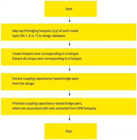
The core of the approach is an ordered listing of bridging hotspots. “These are mapped to the design database and a hotspot zone is defined based on technology parameters of metal spacing and metal width. The nets within the hotspot zone are then used to order bridging pairs from capacitive coupling based bridge pairs.”
The process itself is represented by the algorithm shown in Figure 4.
Figure 4
Bridge pair extraction algorithm
The resulting pairs are then used to generate bridging ATPG patterns, offering an extraction process that is informed more closely by process variation and which should therefore identify potential layout defects in greater numbers.
The team has begun pattern generation based on its technique, which is being validated in silicon.
The work is contained in “DFM-aware bridge pair extraction for manufacturing test development, Poster #12 at the 2010 International Test Conference.


