Implementing DDR3 DIMMs with modern FPGAs
While DDR3 SDRAM offers speed and low-power benefits, the fly-by termination topology defined by the JEDEC specification for DDR3 SDRAM DIMMs creates interesting challenges for FPGAs. The JEDEC topology significantly reduces the simultaneous switching noise that plagues high-frequency parallel interfaces, but also introduces the need for read and write leveling to compensate for the deliberate skew found in the DQ data path.
This article looks at how high-end FPGA I/O cells interface to DDR3 SDRAM to take advantage of these speed and power benefits. It examines how leveling is achieved in the FPGA for operation with a DDR3 SDRAM DIMM; how to use dynamic on-chip termination to alter the impedance on a bidirectional bus and save power; and how to use I/O delay for de-skew within a DQS group.
It also discusses how intellectual property (IP) control algorithms are used in the PHY data path to calibrate the read path at start up and compensate for voltage and temperature variations during operation, enabling the design to reach the highest levels of reliable operation over PVT.
DDR3 SDRAM memory architectures support a higher bandwidth with bus rates of 600Mbps to 1.6Gbps (300 to 800MHz), 1.5V operation for lower power, and higher densities at 90nm. This makes them ideal for a wide range of applications, including servers, storage, LCD displays, networking, and communications equipment.While this architecture is undoubtedly faster, larger, and offers lower power per bit, the fly-by termination topology defined by the JEDEC specification (JESD79-3 for DDR3 SDRAM DIMMs) creates interesting challenges for FPGAs. For example, the topology significantly reduces simultaneous switching noise (SSN), but also requires read and write leveling to compensate for the deliberate skew found in the clock and address/control signals.
This article looks at how high-end FPGA I/O cells interface to DDR3 SDRAM to take advantage of speed and power benefits. It examines:
- how leveling is achieved in the FPGA for operation with a DDR3 SDRAM DIMM memory;
- the benefits of using dynamic on-chip termination (OCT) to match the impedance on a bidirectional bus and save power;
- and the advantages of using variable I/O delay for deskew within a DQS group.
It also discusses the importance of simulating with tools to ensure the best eye quality.
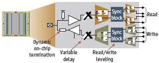
Figure 1. FPGA I/O features for DDR3 SDRAM DIMM memory interfaces
FPGA I/O structures support DDR3
Altera Stratix III FPGAs provide high-speed, flexible support for current and emerging external memory standards, and can interface to DDR3 SDRAM DIMMs. The FPGA I/O structure (Figure 1) has features that enable DDR3 support by addressing signal integrity and timing issues, including read/write leveling, dynamic OCT, variable delay for trace-length mismatch compensation, capture, and half data rate (HDR) capability.
In this I/O structure, memory interface data pins are called DQ pins, while read datastrobes or clocks are called DQS pins. Using a DQS/DQ group for the write data signals minimizes output skew, provides access to the write leveling circuitry, and allows vertical migration. These pins also have access to deskewing circuitry that can compensate for delay mismatch between signals on the bus.
Leveling improves signal integrity
Interfacing to a DDR3 SDRAM DIMM can be complicated and costly, involving numerous external components. To improve signal integrity and support higher performance, the JEDEC specification defines a fly-by termination topology that lowers the number of simultaneous switching signals and improves performance by reducing loading. However, this topology causes flight-time skew between clock and data-strobes at every DRAM as the clock (CK) and address/command signals traverse the DIMM. This flight-time skew can be up to 0.8 tCK, which means that data can be spread over two clock cycles. Clock, address, and control signals daisy chain through a single path across each DRAM in the module because of the fly-by topology. This differs from the DDR2 memory topology, which splits the signal path between each DRAM device through T-branching.
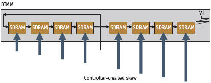
Figure 2. Fly-by termination topology in DDR3 SDRAM DIMMs
To compensate, the specification requires a ‘leveling’ feature when interfacing to DDR3 memories and that controllers are enabled to counteract this skew by adjusting timing per byte lane. Stratix III FPGAs offer leveling that is built into the I/O structure to simplify interfacing to a DDR3 SDRAM device. Leveling should be thought of as more than just I/O delay that appears in the data path: 1T and negative-edge registers are also required to level or align all the data. Figure 2 shows the fly-by termination topology in a DDR3 SDRAM unbuffered module. In this topology, data must be leveled for up to two clock cycles at the controller.
Read leveling
During a read operation, the memory controller side must compensate for the delays introduced by the fly-by memory topology that impacts the read cycle. Each DQS signal requires separate phase shifts of the resynchronization clock position (process, voltage, and temperature (PVT)-compensated). Initially, each separate DQS signal is phase-shifted by a nominal 90 degrees, and the DQ data associated with its group is captured. The free-running resynchronization clock (which is at the same frequency and phase as the DQS signal) is used to move the data from its capture domain into the leveling circuit. At this stage, each DQS group has a separate resynchronization clock.
The resynchronization clock feeds the read-leveling circuitry to produce the optimal resynchronization and postamble clock for each DQS/DQ group in the calibration process. The resynchronization and the postamble clocks can use different clock out puts from the leveling circuitry. The output from the read-leveling circuitry can also generate the half-rate resynchronization clock that goes to the FPGA fabric. Consequently, all output data across the bus can be aligned.
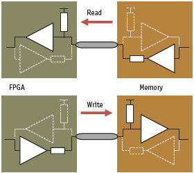
Figure 3. Dynamic OCT: read and write operations
Write leveling
Write leveling is similar to read leveling but reversed. DQS groups are launched at separate times to coincide with the clock arriving at devices on the DIMM. The flight time skew between the clock and strobe makes it difficult to maintain DQS to CK (tDOSS), setup (tDSS), and hold (tDSH).
With write leveling, the controller adjusts the DQS-to-CK relationship by creating a feedback loop in which it writes to the DRAM and reads back. The memory controller involved in the leveling must have an adjustable delay setting on DQS to align the rising edge of DQS with that of CK at the DRAM pin. The Stratix III memory controller uses a built-in calibration algorithm to automatically adjust for the DQS-to-CK relationship depending on the DIMM configuration. The DQS delay thus established ensures that tDOSS, tDSS and tDSH comply with the JEDEC specification.
Dynamic OCT reduces cost and complexity
Dynamic parallel and serial OCTs provide the appropriate line termination and I/O impedance matching capabilities for read and write buses. OCT removes the need for external resistors at the FPGA, improving signal quality and reducing the number of external components, board space, and routing complexity. This feature also significantly reduces power consumption because the parallel termination is effectively out of circuit during write operations. Figure 3 shows dynamic OCT for read and write operations in FPGAs.
The calibration circuitry in Stratix III I/O pins delivers precise control of the impedance value for the OCT resistors over PVT. OCT values are defined in the I/O models. Designers can use simulation software to determine which settings work best for DDR3 designs before committing to a specific board layout.
Variable delay for DQ pin deskew compensates for mismatches
Variable input and output delay can be used for signal duty cycle adjustment and skew compensation due to board trace-length mismatch, simplifying system and PCB design as well as reducing cost. Designers can thereby compensate for any gross trace-length mismatch error. The fine input and output delay resolution (50ps intervals) can be used for more precise inter-DQS deskew (separate from the leveling function) caused by mismatch in board length and variations in the FPGA and memory device. Ultimately, this increases the capture margin for each DQS group.
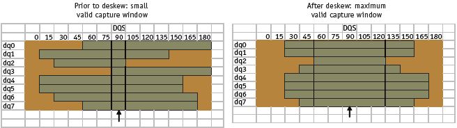
Figure 4. Conceptual DQ deskew within a DQS group centered around 90-degree phase-shifted DQS
The delay elements can be reached from the FPGA fabric at run time allowing the implementation of automatic DDR3 deskew algorithms within the start-up calibration process. The output delay can also be used to insert a small amount of skew into the output path to reduce the number of I/Os being simultaneous switched. Figure 4 shows a conceptual DQ deskew within a DQS group.
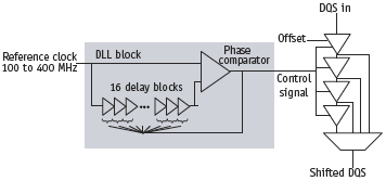
Figure 5. DLL and DQS phase-shift circuitry
Reliable capture maintains optimal phase over PVT
To ensure the highest levels of reliability over PVT, intellectual property (IP) control algorithms are used in the PHY data path to calibrate the read path at start-up and compensate for PVT variations. The DQS signals act as the input strobes and must be shifted to an optimal position for the capture of read transactions, nominally a PVT-compensated 90-degree phase shift. The delaylocked loop (DLL) maintains phase shift in a fixed location across PVT. Figure 5 shows the relationship between the DLL and phaseshift circuitry.
The phase-shift circuitry can shift the incoming DQS signals by 0, 22.5, 30, 36, 45, 60, 67.5, 72, 90, 108, 120, 135, 144, or 180 degrees, depending on the DLL frequency mode. The shifted DQS signals are then used as clocks at the I/O element input registers. The DLL uses a frequency reference to dynamically generate control signals for the delay chains in each of the DQS pins, allowing the DLL to compensate for PVT variations. Stratix III FPGAs offer four DLLs, located in each corner of the device. Each DLL can reach two sides of the device, supporting multiple DDR3 SDRAM memory interfaces on all sides of the device.
High-speed data rate domain crossing simplifies internal timing
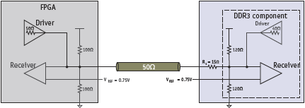
Figure 6. Write operation to DDR3 SDRAM memory using parallel ODT of the DDR3 SDRAM memory and 50? series OCT in Stratix III FPGAs
DDR capture registers and HDR registers allow the safe transfer of data, making the internal design timing much easier to realize. In Stratix III FPGAs, DQ pins feed into an I/O element containing up to 31 registers that are dedicated to interfacing with DDR devices and which support frequencies of up to 400MHz or 800Mbps. Data is transferred from the DDR domain (data on both edges of the clock) to the single data rate (SDR) domain (data on the single positive edge of the clock at the same frequency, but at twice the data width) down to the HDR domain (data on the positive edge of the clock, but the frequency is the SDR frequency and the data width is again doubled).
Before data capture, data changes on both edges of the clock (DDR); after, data changes only on the positive edge of the clock (SDR). An I/O containing an optional-use, second set of datademultiplexing registers can be used to demultiplex the data down to HDR. The data still occurs on the positive edge only, but at half the SDR frequency with twice the data width. HDR is useful if slower and wider data width processes must easily interface with high-speed memory devices.
Simulation improves results
To ensure the best possible results, designers should simulate the interface for eye quality, proper impedance matching, discontinuities, and termination settings.With an EDA simulation tool, the driver and receiver model can be implemented to evaluate the terminations and topologies to be ported for layout. Figure 6 illustrates the read operation from the DDR3 SDRAM memory using the parallel OCT feature of the Stratix III together with the output drive impedance control feature of the DDR3 SDRAM memory. Figure 7 shows a simulation of this operation in Mentor Graphics’ HyperLynx software when the FPGA is writing to memory.
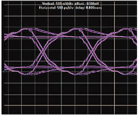
Figure 7. HyperLynx simulation when FPGA is writing to memory
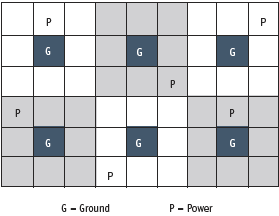
Figure 8. Eight user I/O to each power and ground
Die, package and digital SI enhancements
In addition to the on-silicon features supporting DDR, the die and package design should provide robust signal integrity for highperformance memory interfaces (e.g., an 8:1:1 user I/O-toground- to-power ratio for optimized signal return paths, as in Figure 8). OCT, variable slew rate, and programmable drive strength also help correctly manage signal quality.
Conclusion
Most signal integrity and timing uncertainties that exist when implementing a high-speed DDR3 interface can be addressed by properly supported memory controllers. Designers can establish signal eye quality and additional layout rules by simulating the interface using EDA tools. High-performance FPGAs complement high-performance DDR3 SDRAM DIMMs by providing highmemory bandwidth, improved timing margin, and great flexibility in system design. The combination of FPGAs with DDR3 SDRAM supports the high-throughput requirements of today’s communication, networking, and digital signal processing systems.
Altera Corporation
101 Innovation Drive
San Jose
CA 95134
USA
T: 1 408 544 7000
W: www.altera.com
