Full 3D-IC parasitic extraction
How to enhance an ‘ideal’ parastitic extraction strategy to create a full 3D assembly-level parasitic netlist for simulation and circuit analysis.
3D IC design is gaining a great deal of interest. It promises device scaling at minimized cost within manageable form factors. But there remains the challenge of verifying components produced on multiple processes.
Strides have been taken in the physical verification space. Dies can be verified to specific DRC or LVS rules in standalone mode, allowing the die-to-die interactions to be checked independently in the context of the 3D assembly without requiring process specifics. However, accurate timing analysis and circuit integrity checking are still problematic.
We need a methodology that can describe a multi-process circuit, including intentional device components and parasitics. New technologies under investigation may provide that capability.
Describing and extracting parasitics for an entire system are extremely difficult because at this level the task requires an understanding of the die interconnects. We can normally get connectivity information by running a layout vs. schematic (LVS) comparison, or by reading the connectivity from a routing database like LEF/DEF. However, both techniques are hard to implement across multiple dies, especially in the case of dies from different processes.
Consider the complexity of coding an LVS deck that can properly recognize all the devices, and connect across two dies from different processes (with different foundry LVS decks) that are physically stacked on top of each other. It can be done, but requires significant expertise in LVS rule coding.
There is a way to avoid all this exertion.
Parasitic extraction in an ideal world
In an ideal case, we can assume the most significant parasitic impacts come from the individual die parasitics themselves, and any parasitic impacts between dies are negligible. Presuming parasitic extractions for each die, the only requirement is a method that can stitch together these extracted die netlists.
Using a physical verification tool with 3D verification functionality, like Calibre 3DSTACK, an assembly-level black-box netlist can be extracted and compared against a source netlist. Once this comparison is clean, all that is needed is a way of importing the parasitic netlists from each die to the appropriate black-boxed sub-circuits. The result is a 3D assembly-level, device-level parasitic netlist suitable for various simulations.
This technique works well for designs including through-silicon vias (TSVs), where the TSV can be extracted with the die as a device to be modeled in simulation or as a parasitic model.
But can we really treat the die-to-die and die-to-ball interactions as ideal?
Various coupling interactions can have an impact—for example, microbump/pillar parasitics, ubump to ubump coupling parasitics, couplings between the bumps and the top routing layers of the die, and even possible coupling between the top routing layers of two stacked dies. To capture these interactions, the previous approach is insufficient. Yet with perhaps a bit more effort, we can extend it.
Enhanced parasitic extraction strategies
Two strategies can help us improve the level of parasitic extraction accuracy without imposing the need for a monolithic assembly-level extraction.
Under the first, we extract the interfaces separately, and then stitch these parasitics at the assembly level to the die-level parasitics for the sub-circuits. Alternatively, we extract all the die placements ‘in context’, meaning they are extracted with knowledge of the interface layers with which they interact in the context of the assembly.
Using the second approach, all the dies are extracted in context. However, we must identify the individual die placements that own the interface parasitics. For those dies, the interface parasitics are netlisted together with the parasitics of the original dies. For the other dies, the impact of the interface(s) is lumped into the parasitics of the die’s top layer(s) to avoid double counting.
To enable such a parasitic extraction, we must include enough data about geometries and materials from neighboring placements with the die’s placement (Figure 1). By incorporating the interface layers of interest into the bottom die, we can capture the interface parasitics, and the parasitics to the interposer and middle die geometries. Similarly, by combining the interface layers between the top two dies with the top die, and the interfaces around the middle die with the middle die, we can capture the parasitics of those interfaces. To avoid double counting, the middle die should be netlisted without including the interface parasitics, and the impact of the interfaces should be lumped into the middle die’s top layer and backside outmost-layer parasitics.
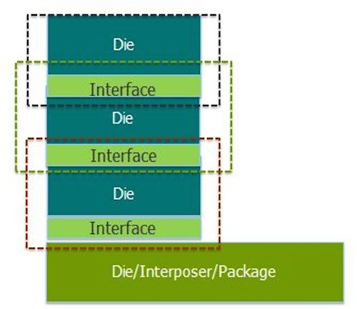
Figure 1. A 3D-IC package shows how interfaces between dies are grouped with the dies (Source: Mentor Graphics)
We can create a new layout representation of a die that includes layers of interest from the interfaces and appropriate neighboring die layers, such as one or two top-level routing layers, in the primary die layout. With this new layout, and a modified parasitic calibration that takes into account both the interfaces and the additional layer dielectric properties and vertical distances, we can perform a new parasitic extraction capturing both the internal die parasitics and the parasitics of the interfaces. Of course, coupling parasitics from the neighboring die geometries must be modeled as lumped parasitics.
This approach does require more effort than the ideal case.
First, extracting these parasitics requires an updated calibration for the dies to include the dielectric properties and thicknesses in the interfacing regions. This task may be simplified though by incrementally adding to an existing process calibration for a given die.
Second, to enable a device-level extracted netlist, we must perform a new LVS for the modified layout that includes the new interconnect materials. Fortunately, adding interconnects to a process LVS deck is relatively simple and process-independent, since no intentional devices from the neighboring dies must be captured.
Finally, to create a 3D stack top netlist using the in-context methodology, we must move the ports of the interface(s)-owning dies to the other side of the interfaces.
With this approach, we can now capture the die-to-die coupling parasitics per die. Using the same techniques employed for the ideal case, we can import these parasitics into the assembly-level netlist, resulting in a full 3D assembly-level parasitic netlist suitable for simulation and circuit analysis.
About the authors
John Ferguson is the Director of Marketing for Calibre DRC Applications at Mentor Graphics. He has extensive experience in the area of physical design verification. John holds a BS degree in Physics from McGill University, an MS in Applied Physics from the University of Massachusetts, and a PhD in Electrical Engineering from the Oregon Graduate Institute of Science and Technology.
Dusan Petranovic is an Interconnect Modeling Technologist with the Design to Silicon group at Mentor Graphics, working on all aspects of parasitic extraction. Dusan received a BSEE from the University of Belgrade, an MS from Worcester Polytechnic Institute, and a PhD from the University of Montenegro, where he was a professor and chairman of the EE department. He also taught at Harvey Mudd College, and worked for LSI Logic’s Advanced Development Laboratory, NASA, and NOVA Management, Inc. Dusan holds fifteen US patents and has published numerous journal and conference papers.
Contact
Mentor Graphics
Corporate Office
8005 SW Boeckman Rd
Wilsonville
OR 97070
USA
T: +1 800 547 3000
W: www.mentor.com
