From algorithm to first 3.5G call in record time
Increasing system complexity is forcing design teams to avoid errors during the process of system refinement and reduce ambiguities during system implementation to a minimum. On the other hand, the system design approach they choose must enable a project to advance rapidly through all stages of refinement from an algorithmic model to a real system-on-chip (SoC) while maintaining backwards equivalence with the hardware (HW) and the firmware/software (FW/SW) code from that original algorithmic model. This challenge demands the use of a new interdisciplinary team approach encompassing all design skills ranging from concept to HW and FW/SW engineering as well as system verification. How are we to enable these interdisciplinary teams to cooperate efficiently, given that they are used to “speaking different design languages”?
This paper outlines a novel system design strategy that was used on a project which set an industry record for the development time of a 3.5G UMTS modem. The framework provided a common system design language and avoided the Babel-like muddle through which different engineering worlds can become isolated.
The motivations for an increasing the overlap between the system concept, implementation and verification phases are obvious. Greater design flow integration can shorten time-to-market by several months, by allowing the parallel development of HW and FW/SW. It also helps engineers to avoid costly redesign cycles due to conceptual errors and optimizes the quality of the developed system HW and FW/SW thereby also substantially reducing system development R&D costs.
The process of turning a system concept into a complex SoC system has always entailed multiple stages of abstraction, detailing the hardware-firmware/software (HW-FW/SW) split and adding detail to the implementation. System refinement continues until a project reaches a synthesizable representation of the SoC that can be compiled into a netlist for semi-custom HW design and a code image running on an embedded microprocessor core.
This iterative process of refinement and decomposition (often referred to as a ‘V-model’) can only be successful if it employs a seamless approach to system modeling. It must guarantee that errors during refinement into HW and FW/SW are kept to a minimum and that implementation ambiguities are avoided, because both are likely to result in system malfunctions. Modern design flows are not yet entirely capable of generating optimized synthesizable HW and executable FW/SW code for complex embedded SoCs from highlevel algorithmic system descriptions. Nevertheless, an algorithmic system model can be used as a reference for verification against RTL code and ideally should also be reused in a virtual prototype (VP) on which embedded FW/SW can be developed.
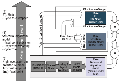
Figure 1. HW – algorithm model co-simulation of Rake receiver
Based on this conclusion, a seamless system design flow can be established and is here demonstrated. This flow has significant consequences for the creation of cross-functional design teams. It literally represents a common language through which concept, HW and FW/SW engineers communicate and collaborate. In essence, it unifies a development strategy that was previously decomposed.
Virtual prototypes (VPs) have been successfully deployed on many microprocessor-centric system designs (e.g., application processors for mobile phones). However, for signal-processing dominated systems, the challenge of integrating models of the algorithm into a VP also has to be addressed. This paper specifically considers a 3.5G modem design where such algorithm models were tightly integrated into the system VP and co-simulated against the hardware RTL code using slave simulation techniques.
From algorithm to hardware
Meeting the performance specification (e.g., the 3GPP specification) is the key requirement for a 3.5G modem. To do so, the entire receiver and transmitter system has to be modeled and simulated to demonstrate that its algorithms meet – or better still, exceed – the relevant standards. Concept engineers first developed our model and we then deployed a communication systems simulator (SystemStudio) based on an abstract algorithm modeling language. An analysis of which algorithms best meet specification requirements for, say BLER and SINR, is most effectively carried out at this high system-description level.
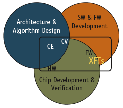
Figure 2. The concept of cross-functional teams
The algorithm model does not have to be cycle-accurate, unlike a synthesizable HW RTL description. Yet the two representations for the different abstraction levels do have to be equivalent with respect to the processed data. We resolved this apparent contradiction by having the HW and concept engineers cooperate and work on a HW model co-simulation that provided this proof of equivalence.
For the modem, this was achieved by adding detail to the algorithm model at an abstraction level that allowed the RTL code to be compared against it at slot-level timing resolution (a 10ms UMTS frame consists of 15 slots). Not only was timing information added to the algorithm model but it also was refined from floating to fixed-point precision (Figure 1). As a result, the HW and concept engineers were able to co-simulate the RTL and algorithm models based on a single schematic, thus establishing an automated pass/fail criterion for chip sign-off regression testing.
Project management
In the previous section, we described a team consisting of groups with different skill-sets (namely, algorithm or concept engineers (CE) and HW designers) that needed a shared strategy to enable thorough co-simulation. Needless to say, a co-simulation also requires FW/SW input for HW configuration and status evaluation.
For our 3.5G modem, the concept was extended by setting up cross-functional teams (XFTs) in which all the aforementioned disciplines were represented, and which was completed by a fourth group that handled system verification (CV).
The various groups in an XFT (Figure 2) usually have differing backgrounds (e.g., HW design usually requires a knowledge of RTL; FW/SW engineers work in real-time embedded SW design environments), yet they all share a familiarity with programming and simulation techniques. Therefore, making an XFT successful requires a common denominator – or better still, a common language – which describes the system behavior at the desired abstraction level and allows FW/SW to be developed on an abstracted model of the HW before engineering samples are available. A virtual prototyping strategy serves this purpose ideally.
A detailed model for FW/SW design
For the 3.5G modem, a VP (Figure 3, p.16) was developed on the basis of offering maximum re-use potential, using existing building blocks from the SystemStudio algorithm simulation chain. These signal processing peripheral models were wrapped with SystemC and integrated with SystemC models of the chip’s control blocks. Re-using identical models in the VP as were used for HW verification ensured consistency between the VP and the target HW. A fast instruction set simulator completed the VP.
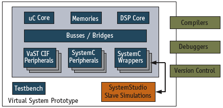
Figure 3. Virtual system prototype (VP)
An easy-to-use stimulus/response mechanism was essential to the prototype’s development. It represented both the basestation (Node B) and the host (comprising the higher layers of the 3.5G protocol stack). Details of the testbench implementation for the 3.5G basestation (Node B) and the host were ‘hidden’ for the users (testers) and accessible via an easy-to-use API and encapsulated testbench libraries.
The testcases developed on the VP were designed for reuse during silicon verification without major changes. This added value by enabling a fast characterization of the HW and allowed for easy porting and verification of FW/SW developed on the VP on the target system HW. The entire VP was fully transparent and could be suspended/resumed in system verification to ease debugging. This was a major advantage over the target system HW. Hence, incremental FW/SW design with source code level debuggers attached to the 3.5G modem model could continue on the VP even after the first silicon was available.
As the FW/SW development design was carried out incrementally, so was the VP design. The advantage of this was that the VP did not have to be complete from the very beginning (nor did the system testbench) but rather could grow incrementally as system requirements allowed or required it. For example, 3G ‘Compressed Mode’ functionality was only added late on (and consequently to the 3G basestation stimulus), as it was not necessary for basic call setup system simulations.
Results
A comparison of the system design approach with a conventional (i.e., sequential) approach using classical RTL design and FPGA prototyping has to consider what savings were achieved on the project schedule as a result of the effort invested.
The VP approach allowed for incremental development of the modem’s system FW/SW shortly after the design concept was ‘frozen’ (in fact, the VP was developed concurrently with the system concept to also form a ‘proof of concept’). The alternative would have been a full FPGA-based system prototype that would have required an almost complete RTL system representation (after synthesis and verification). Due to the size and complexity of the 3.5G modem, an FPGA prototype would have also required system partitioning onto several FPGAs. By avoiding these steps and because of the availability of a system VP, the HW-FW/SW integration started about six months earlier than would otherwise have been possible.
The developed 3.5G modem HW was ‘first time right’. Only two weeks after HW availability the first FW/SW builds were ported onto the target HW. Some 18 months after system design on the project began, the first call over a live 3.5G network took place and functionality of the high-speed downlink packet access (HSDPA) protocol was demonstrated.
Many VP building blocks are necessary and hence available for a complex system setup anyway (e.g., the algorithm models that constitute the receiver & transmitter of the modem). The extra effort came in adding SystemC models to complete the VP, the system bring-up, and initial verification of the VP. Together with maintenance, these efforts amounted to approximately six man-years, although we are sure that this kind of figure will decrease as the methodology matures. Moreover this R&D investment in VP technology is already being reused on other projects and a design framework (called SysWay) has been set up based on our successful experience with virtual prototyping.
The employment of the VP also saved budget items such as expensive 3.5G signal generators and FPGA systems, which would otherwise have been required for most of the FW/SW development phase.
Summary and outlook
This VP-based approach to system design has greatly increased the productivity of our design teams working on complex embedded SoCs. A VP is an extremely useful common system model because it can be used by concept, HW and FW/SW designers. In particular, it cuts design cycle time by creating a greater overlap between the concept, implementation and verification phases of complex projects.
As this VP methodology matures into more mainstream system flows, it will offer increasing benefits in the area of high-level architecture exploration, and its strengths become especially apparent during the system refinement phase. Additionally HW verification is easily imaginable in the full VP context (e.g., replacing individual algorithmic blocks by the corresponding HW) instead of standalone co-simulation with the algorithm models.
For wireless communication systems, minimizing power consumption is becoming increasingly important, and we believe the modeling of this key system requirement will soon also find its way into VP-based strategies.
Infineon Technologies AG
Development Center Münche
Am Campeon 1-12
D – 85579 Neubiberg
Germany
T: +49 89 234 0
W: www.infineon.com
