The five key challenges of sub-28nm custom and analog design
The arrival of the 20nm and finFET-based 14nm and 16nm processes bring with them challenges for custom IC design. These are the five key areas and a methodology that can address them.
The new generation of 20nm and sub-20nm process nodes offer greatly improved circuit density and power/performance characteristics. At the same time, they raise new concerns for SoC integration, particularly with respect to mixed-signal and custom design flows. At 20nm and below, an increased amount of silicon IP must be obtained from multiple sources, and there will be increasing concerns about mixed-signal design, integration, and verification. Mixed-signal interactions will increase as more and more digital control circuitry is used, and as analog and digital components come into close proximity.
Of most concern to custom/analog designers are the challenges that arise from manufacturing complexity. On top of increasing timing, power, and area challenges, the 20nm process generation brings with it the deep and complex interdependency of manufacturing and variability. The five main challenges of 20nm custom and analog design comprise the use of double patterning; layout-dependent effects (LDE); the use of new types of local interconnect layers; a massively increased collection of design rules; and increasing device complexity and variation. Concerns about manufacturability issues vary according to design style. For example, analog and I/O designers are most concerned about LDE, circuit specifications, and area versus performance tradeoffs. Memory and standard cell designers are very concerned about density, and as such, double patterning and local interconnect are key concerns.
The solution to 20nm custom/analog challenges lies not only in new point tools, but in a new custom design methodology. In this methodology, circuit (schematic) and layout designers will work in close collaboration, and will have the ability to rapidly exchange information. Circuit designers will be able to obtain early parasitic estimates before the layout is completed. The flow will use in-design, signoff-quality engines as opposed to attempting to fix everything during the final signoff stage. And all tools will be “double patterning-aware” and ready for 20nm.
1. Double Patterning
The most-discussed manufacturability issue at 20nm is double patterning. This technology splits a layer into two separate masks so that 193nm lithography can print structures that are too close together to resolve with a single mask. This technology is needed to get current 193nm lithography equipment to print correctly when metal pitches are below 80nm, which will be the case for at least some of the metal layers for almost any 20nm design.
When double patterning is used, each mask is exposed separately, and the exposures overlap to create features that are half the pitch that would otherwise be printable with 193nm lithography.
The concept may be simple, but managing double patterning is difficult. It requires a two-color layout decomposition process in which alternate colors (such as red and green) are used to indicate which features will be placed on which mask. This results in added design rules that restrict the placement and proximity of layout features. For example, traces that are the same color can’t be placed too closely together.
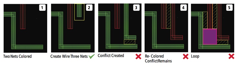
Figure 1 Attempts to solve double patterning issues can easily lead to loops
It is very easy to create a design-rule checking (DRC) “loop,” which is a coloring conflict that cannot converge on a solution that works. And in many cases, it will be necessary to trace back a number of steps to unravel how the loop was created.
Handling double patterning properly is a major concern for custom designers of standard cells, memories, and I/Os. These designers must be cognizant of coloring as they create layouts to optimize area. It is difficult to achieve a high density while making the design decomposable. According to some reports, standard cells that previously took four hours to lay out sometimes take a week at 20nm, because designers have to keep re-running verification as they try to pack decomposable cells as tightly as possible.
Analog designers are concerned about the mismatches that an additional mask can cause. Double patterning impacts electrical performance because different masks on a given layer will shift during the manufacturing process. This mask shift causes variations that have a direct impact on RC and the interconnect. As a result, parasitic matching can become very challenging between elements that are rendered using different masks.
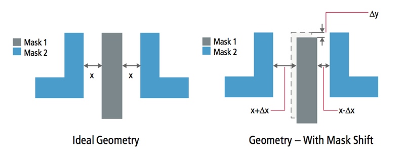
Figure 2 Mask shifts can occur with double patterning
EDA tools can help automate the colorized decomposition process and can help ensure correctness. In a 20nm-aware toolset, all physical design tools should be double patterning‒aware, including placement, routing, extraction, and physical verification. For example, extraction must be able to predict the capacitance variation resulting from mask shift.
Another capability that’s needed is automated color-aware layout. Here, color conflicts are avoided as the layout designer draws shapes and places cells. Once a shape is dropped into place, the tool automatically makes any needed coloring changes. Locking color choices down in the design phase sets a constraint for the manufacturer and helps to ensure that matching is correct by placing pairs of nets or devices on the same mask.
Instead of running signoff verification once every four hours, a quick double patterning check should be run after every editing command. In this way errors can be fixed quickly, and designers don’t end up with DRC loops that may take many steps to unwind.
2. Layout-Dependent Effects
At 20nm, it’s not enough to model the performance of a transistor or cell in isolation. The environment around a device will change its behavior, a phenomenon captured by the term LDE. Although LDE became apparent at 28nm, the problem has grown significantly worse at 20nm, where cells are much closer together. At 20nm, up to 30 per cent of device performance can be attributed to the layout ‘context’. For example, the voltage threshold of a transistor will change based on how close the device is to the edge of a well – this is called the well proximity effect.
Other modifiers of device performance include the distance between gates – including dummy poly – which has a direct effect on the drain current of the transistor. This is known as the poly spacing effect. Another major cause of LDE is mechanical stress, which is often intentionally induced to improve CMOS transistor performance. For example, a dual stress liner is a silicon nitride (SiN) capping layer that is intentionally deposited to be compressive on PMOS and tensile on NMOS. Such stresses improve the performance of either form of transistor. Nonetheless, it results in variability that may make it difficult to close timing. Stress is also unintentionally induced through technologies such as shallow trench isolation, which isolates transistors and determines active-to-active spacing.
LDE cannot be modeled in Pcells (parametized cells) or device models. As a result, it is no longer enough to create a schematic, pick a topology, run a simulation, and throw it over the wall to a layout designer. At 20nm, circuit designers have to consider layout context as well as device topology, and they need to simulate with layout effects prior to layout completion. This may sound paradoxical, but it is possible to identify devices that are sensitive to LDE and thus allow the designer to recognize which components need greater care in layout. Less sensitive devices can be placed closer to well boundaries, for example. Circuit designers can also make use of LDE simulation using partial layouts and LDE-aware layout module generators. Layout engineers can use LDE hotspot detection and fixing.
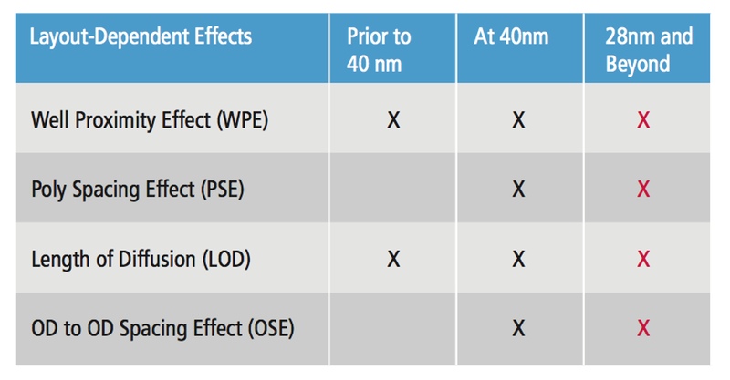
Figure 3 The increase in layout-dependent effects with reductions in geometry
The underlying technology that is needed is context-driven placement and optimization that can determine how different cells are going to interact and how the layout context affects timing and power. The design tool should take care of LDE during both schematic and layout phases. But it’s not just about tools. Circuit and layout designers have to learn to work together in new ways, with a much higher level of cooperation.
3. Interconnect layers
For many custom designers, 20nm is all about density. Local interconnect (LI) layers – also called middle-of-line (MOL) layers – offer a way to achieve very dense local routing below the first metal layer. There may be several of these layers available in a given process, and most don’t use contacts. Instead, they connect by shape overlap without any need for a cut layer. Getting rid of contacts makes routing denser because contacts are bigger than nets, and can’t be placed too close to nets.
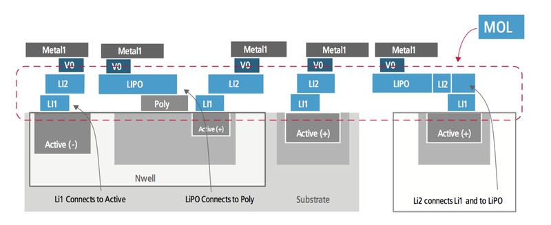
Figure 4 New types of local interconnect enable increased density at 20nm
However, designers need to be aware that LI layers have their own restrictive design rules. For example, LI shapes can only be rectangles, and they often have fixed directions with length constraints.
4. Design rules
At 20nm, there may be more than 5,000 design rule checks. Some 1,000 new rules have been added since the 90nm process node, and double patterning alone requires 30 to 40 checks. The 20nm node adds another 400 new advanced rules such as wrong width and wrong spacing, discrete width and spacing, and special rules for pin access on cells. Custom and mixed-signal designers will face directional orientation rules, specific rules regarding length/width and transistor proximity, and new rules governing legal inter-digitation patterns.
An important point to remember is that 20nm doesn’t just bring in more rules; it brings in more complex rules. Simple rules of thumb or memorization won’t work any more. What’s needed is a design system that can check design rules as the design progresses, rather than waiting for a final signoff check.
5. Device complexity and variation
Transistors at 20nm are very small and very fast, and variation is a constant challenge. Transistors are sensitive to channel length and channel doping, and transistor behavior is subject to short-channel effects. Custom designers must minimize leakage, ensure reliability, and achieve reasonable yields.
The reality is that 20nm transistors were designed for achieving high densities in digital design, not for optimizing leakage or gain in custom/analog design. A limited set of device sizes are available for design. Width and length parameters are limited to a small set of values, and with fewer choices, manually tuning transistors to meet specs (such as gain) is difficult.
Below 20nm many, if not most, designs will use a new type of transistor called a FinFET. In a FinFET, the transistor gate wraps around three sides of the transistor’s elevated channel, or ‘fin’. This forms conducting channels on three sides of the vertical fin structure, providing much more control over current than planar transistors. Multiple fins can be used to provide additional current. FinFETs promise greatly reduced power at a given level of performance.
However, FinFETs raise some challenges for custom/analog designers. One constraint is that all the fins on the transistors on a given chip must be the same width and height. Designers can add fins to increase the width, but this can only be done in discrete increments—you can add 2 fins or 3 fins, but not 2.75 fins. In contrast, planar transistors can be adjusted to any channel width in order to meet specifications.
Other challenges include additional design rules, manufacturing variations in the width and height of fins, and metal and via resistance. SPICE models with additional parameters will be needed for the FinFETs, and simulators must be able to interpret them. Extraction tools must be aware of the capacitance and resistance that arises from 3D transistor structures. Layout tools will have to be optimized to handle FinFETs. And like any new technology, FinFETS will require ecosystem support including EDA tools, process design kits (PDKs), physical IP, and silicon-proven manufacturing processes.
A new methodology
To resolve the challenges described in the above sections, every tool in the custom/analog flow needs to be aware of the changes that 20nm brings, including double patterning, LDE, local interconnect, complex design rules, device variation, and FinFETs. But it is not enough to just improve tools. What is needed is a new methodology that provides a higher level of automation than existing flows. In this methodology, circuit and layout designers will exchange and share information, ”partial layout” will provide early estimates of parasitics and LDE, and an in-design signoff approach will greatly shorten final signoff runs.
The traditional custom/analog flow is a manual, “throw it over the wall” approach. Circuit designers do schematic entry and run an ideal simulation without layout parasitics. The design is tossed to layout designers who handle device creation, manual placement, and manual routing. Next comes physical verification, extraction, and a final simulation. It’s a time-consuming, serial methodology in which issues are exposed very late in the design process, and many design iterations may occur. Without changing this approach, blocks that took four hours to lay out at 28nm could easily take a week at 20nm.
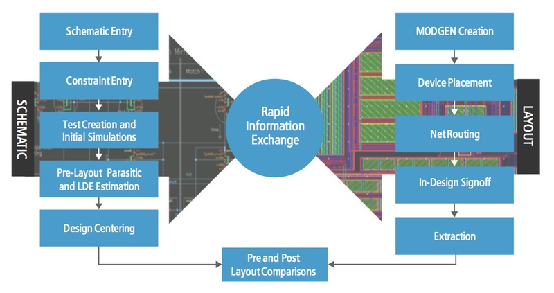
Figure 5 A sub-25nm custom design methodology allows rapid information exchange between schematic and layout
What is required is a more automated and collaborative methodology. Here, circuit designers draw schematics, just like they always have. But they also pass constraints to the layout designers, and run a pre-layout parasitic and LDE estimation. On the right side of the diagram, both circuit designers and layout designers can use Modgens – a Cadence term for automatic module generators – to quickly generate layouts for structures such as differential pairs, current mirrors, and resistor arrays. Although not final “DRC-clean” layouts, these automatically generated layouts allow accurate physical effects to be extracted, analyzed, and simulated. Modules can then be fed into an analog placer and assembled into a floorplan.
Layout engineers then perform device placement, routing, in-design signoff, and extraction. In short, the basic roles of circuit designers and layout designers remain the same, but there is an ongoing and rapid exchange of information and a high degree of collaboration. Constraints flow easily between the schematic and layout environments.
Automatic module generators help enable “partial layout,” which is the ability to quickly generate an extracted layout view so circuit designers can run simulations with real parasitic and LDE information. In this way, the electrical and mismatch problems that might be caused by layout effects can be spotted and remedied early in the design cycle. The module generators, however, must be ready for 20nm, with place-and-route engine support for 20nm design rules, complex abutment support, array-based FinFET configurations, coloring for double patterning, and LDE awareness.
Another approach for bringing physical effects into initial simulations is incremental design. Here, designers lay out the pieces they care about with assisted or full automation, and gather as much physical and electrical information as they can. This results in a partial layout extraction. The emphasis is on placement rather than routing. The point is that designers are not taking the time to do a full layout, just what’s necessary to generate the desired parasitic information.
Finally, in-design signoff is a must at 20nm. If a designer makes a mistake during layout, the feedback should come immediately, not four hours or a month later. Otherwise many design iterations may be needed for each block, with each iteration taking longer than it took to do the original design. There are two types of interactive editing checks that can help avoid those iterations. One is “in-edit checking,” which warns of errors while geometry is being created. Another is “post-edit signoff-quality checking,” which exercises a more robust check after each edit is completed.
The key to in-design signoff is having “signoff-quality” engines that run during the design flow. This does not remove the need for a final signoff check, but it greatly reduces the amount of time and potentially the number of licenses that a final check might consume.
Conclusion
The performance, power, and density advantages of the sub-25nm nodes will provide competitive advantages to those who adopt them. Although there are a number of design and manufacturing challenges, the good news is that the challenges are manageable – but only if we look beyond individual tools and rethink the ways that custom and analog circuits are designed.
What’s needed is a new custom/analog methodology in which schematic and layout designers work in close cooperation, schematic designers can run prototype layouts to gather parasitic and LDE information, and signoff- quality engines permit “in-design signoff” that catches the vast majority of errors before the final signoff phase. Cadence Design Systems fully supports such a methodology today.
About the author
Steve Carlson is marketing group director for silicon realization at Cadence Design Systems.
Contact
Cadence Design Systems
2655 Seely Avenue
San Jose, CA 95134
T: +1 (408) 943 1234
W: www.cadence.com
