Destination network-on-chip
The network-on-chip (NoC) design paradigm is seen as a way of enabling the integration of an exceedingly high number of computational and storage blocks in a single chip. But its adoption and practical implementation face important and unsolved issues related to design methodologies, test strategies, and dedicated CAD tools.
The System-on-a-Chip Research Lab at the University of British Columbia has taken its existing experiences of SoC design, verification and test to launch its own NoC project. It is proving to be one of the most ambitious projects undertaken by the group.
Interconnect
As a result of the increasing degree of integration now possible in silicon and required for NoC, several research groups are striving to develop efficient on-chip communication infrastructures.
There already exist many SoC designs that contain multiple processors for applications such as set-top boxes, wireless base stations, HDTV, mobile handsets, and image processing. Following on from this, new trends in the design of communication architectures in multi-core SoCs have appeared in recent research papers.
Some suggest that multi-core SoCs can be built around different but regular interconnect structures that have their roots in architectures used for parallel computing. Custom-built applicationspecific interconnect architectures are also promising.
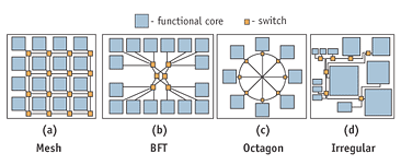
Figure 1. Proposed NoC Interconnect templates
Such communication-centric interconnect fabrics are characterized by different trade-offs with regards to latency, throughput, reliability, energy dissipation, and silicon area requirements. The nature of the application will dictate the selection of a specific template for the communication medium. To give a sense of the alternatives now being tabled, Figure 1 below shows a representative set of interconnect templates proposed by different research groups. A complex SoC can be viewed as a micronetwork of multiple blocks, and hence, models and techniques from networking and parallel processing can be borrowed and applied.
For NoC, the micronetwork must meet quality of service requirements (such as reliability, guaranteed bandwidth/latency), and deliver energy efficiency. And it must do this under the limitation of intrinsically unreliable signal transmission media. Such limitations are due to the increased likelihood of timing and data errors, the variability of process parameters, crosstalk, and environmental factors such as electro-magnetic interference (EMI) and soft errors.
To address these tasks, current simulation methods and tools can be ported to networked SoCs to validate functionality and performance at various abstraction levels, ranging from the electrical to the transaction levels. NoC libraries, including switches/routers, links and interfaces will provide designers with flexible components to complement processor/storage cores. Nevertheless, the usefulness of such libraries to designers will depend heavily on the maturity of the corresponding synthesis/ optimization tools and flows. Efficient micronetwork synthesis is needed to enable NoC/SoC design much as logic synthesis enabled efficient semicustom design in the 1980s.
Though the design process of NoC-based systems borrows some of its aspects from the parallel computing domain, it is driven by a significantly different set of constraints. From the performance perspective, high throughput and low latency are desirable characteristics of multi-processor SoC platforms. However, from a VLSI design perspective, the energy dissipation profile of the interconnect architectures is of prime importance as the latter can represent a significant portion of the overall energy budget. The silicon area overhead due to the interconnect fabric is important too.
The common characteristic of these kinds of architectures is such that the processor/storage cores communicate with each other through high-performance links and intelligent switches and that the communication design can be represented at a high abstraction level. The exchange of data among the processor/storage cores is becoming an increasingly difficult task with growing system size and nonscalable global wire delay. To cope with these issues, the end-to-end communication medium needs to be divided into multiple pipelined stages, with delay in each stage comparable with the clock-cycle budget.
In NoC architectures, the inter-switch wire segments together with the switch blocks constitute a highly-pipelined communication medium characterized by link pipelining, deeply-pipelined switches, and latency-insensitive component design.
Test
A methodology can only be widely adopted only if it is complemented by efficient test mechanisms. Developing such an infrastructure for the NoC paradigm is a serious challenge.
Specifically, the design of specialized Test Access Mechanisms (TAMs) for distributing test vectors and novel Design for Testability (DFT) schemes assume major importance.Moreover, in a communication-centric design environment like that provided by the NoCs, fault tolerance and reliability of the data transmission medium are two major requirements in safety-critical applications.
The test strategy of NoC-based systems must address three problems:
1. Testing of the functional/storage blocks and corresponding network interfaces. 2. Testing of the interconnect infrastructure itself. 3. Testing of the integrated system.
For testing the functional/storage blocks and their network interfaces a TAM is needed to transport the test data. It transports test stimuli from a test pattern source to the core under test. It also transmits test responses from the core under test to test pattern sink. There is a major advantage in using NoCs as TAMs, specifically an ability to reuse the existing resource and the availability of several parallel paths to transmit test data to each core. Thereby, system test time can be reduced through the extensive use of test parallelization (i.e. more functional blocks can be tested in parallel as more test paths are available).
The controlability/observability of NoC interconnects is relatively reduced because they are deeply embedded and spread across the chip. Pin-count limitations restrict the use of I/O pins dedicated to test of the different components of the data-transport medium. So, the NoC infrastructure should be progressively used for testing its own components in a recursive manner (i.e. the good, already tested NoC components should be used to transport test patterns to the untested elements).
This strategy minimizes the use of additional mechanisms for transporting data to the NoC elements under test, while allowing reduction of test time through the use of parallel test paths and test data multicast.
Testing the functional/storage blocks and the interconnect infrastructure separately is not sufficient to ensure adequate test quality. The interaction between the functional/storage cores and the communication fabric has to undergo extensive functional testing. This functional system testing should encompass testing of I/O functions of each processing element and the data routing functions.
Reliability
Many SoCs are used within embedded systems, where reliability is a figure of merit. At the same time, beyond the 65 nm node, transistor and wire failures are more likely to happen due to a variety of effects, such as soft (cosmic) errors, crosstalk, process variations, electromigration, and material aging.
In general, we can distinguish between transient and permanent failures and the design of reliable SoCs must encompass techniques that address both types.
From a reliability point of view, one of the advantages of packetized communication is the possibility of incorporating error control information into the transmitted data stream. Effective error detection and correction methods borrowed from fault-tolerant computing and communications engineering can be applied to cope with uncertainty in on-chip data transmission. Such methods need to be evaluated and optimized in terms of area, delay and power trade-offs.
Permanent failures may be due to material aging (e.g. oxide), electromigration and mechanical/thermal stress. Failures can incapacitate a processing/storage core and/or a communication link. Different fault-tolerant multiprocessor architectures and routing algorithms have been proposed in the parallel processing domain. Some can be adapted to the NoC domain, but their effectiveness needs to be evaluated in terms of defect/error coverage versus throughput, delay, energy dissipation and silicon overhead.
Network interfacing
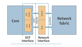
Figure 2. Interfacing of IP cores with network fabric
The success of the NoC design paradigm then relies greatly on the standardization of the interfaces between intellectual property (IP) cores and the interconnection fabric. Using a standard interface should not impact the methodologies for IP core development. In fact, IP cores wrapped with a standard interface will exhibit a higher reusability and greatly simplify the task of system integration . The Open Core Protocol (OCP) is a plug and play interface standard receiving wide acceptance. As shown in Figure 2 below, for a core having both master and slave interfaces, the OCP-compliant signals of the functional IP blocks are packetized by a second interface. The network interface has two functions:
1. Injecting/absorbing the flits leaving/arriving at the functional/storage blocks, 2. Packetizing/depacketizing the signals coming from/reaching to OCP compatible cores in form of messages/flits.
All OCP signals are unidirectional and synchronous, simplifying core implementation, integration and timing analysis. The OCP defines a point-to-point interface between two communicating entities, such as the IP core and the communication medium. One entity acts as the master of the OCP instance, and the other as the slave. OCP unifies all inter-core communications.
You can find out more about the UBC SoC lab’s research at soc.ece.ubc.ca.
