Designing a PCB for power integrity
Signal integrity (SI) issues have been around for a while, the result of ever-faster edge rates. Both SI and PI problems manifest themselves as data errors. Indeed, PI problems are often misdiagnosed as SI problems. As such, an understanding of power delivery issues is essential to the success of any board project, as is a willingness to deal with these issues early in the design flow.
Power integrity (PI) is an increasingly complex problem in higher-end electronic product designs. A few years ago, all ICs ran at 5V; single 5V and GND layers were all you needed to deliver sufficient, clean power to the components. ICs today run at multiple—and much lower—voltages, down to 0.9V.
Figure 1 shows a contemporary IC with multiple voltages and the complex power distribution networks (PDN) required to supply the voltages and grounds. Several factors contribute to increasing PCB design complexity for both CAD designers and engineers who analyze these PDNs. They include a growing number of different voltages; smaller voltage magnitudes (resulting in very tight tolerances); rising power demands from ICs; increasing operating frequencies; and ongoing pressure to control product cost (e.g., you can no longer afford to devote a PCB layer to every unique voltage and ground).
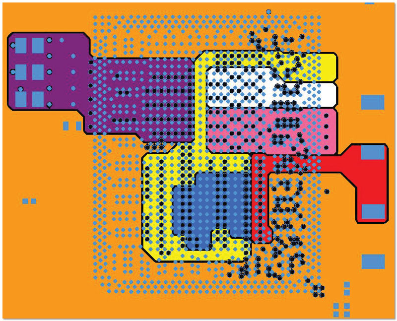
Figure 1
This IC requires six voltages, each fed by a separate PDN
Signal integrity (SI) issues have been around for a while, the result of ever-faster edge rates. Both SI and PI problems manifest themselves as data errors. Indeed, PI problems are often misdiagnosed as SI problems. As such, an understanding of power delivery issues is essential to the success of any board project, as is a willingness to deal with these issues early in the design flow.
The CAD designer challenge
The basic challenge for the CAD designer is to create PDNs that feed from the voltage regulator modules (VRMs) that supply all the ICs (with their various voltages or grounds) on the fewest number of PCB layers. The good news is that defining a PDN is a highly automated process in more advanced PCB layout systems, one example being Expedition Enterprise from Mentor Graphics. Simply outline the PDN shape and the software floods the area. The bad news is that these PDNs must typically be ‘jigsawed’ into the fewest number of layers. Designs can contain more than 30 PDNs, so a designer can face a very daunting situation.
Even after the PDN layout is complete, CAD designers must either perform PI analysis themselves or work closely with electronics engineers to ensure that sufficient, clean power is being delivered to all ICs. Corrections may require changes to PDNs and/or the placement of capacitors on the PCB.
Parasitics and impedances
From the electrical point of view, the goal in designing a PDN is simple to describe: minimize the impedance between power and ground for the appropriate frequency range. The successful execution of that goal is not so simple. Complexity is inevitable when there are multiple voltage rails and a limited number of planes available to carry those voltages, while the real estate available for capacitors on a PCB is shrinking all the time.
The PDN comprises the combination of DC-to-DC-converter VRMs supplying voltage to the rail; decoupling capacitors tied between power and ground; planes and/or traces carrying power; on-chip decoupling; and pins and vias that connect these elements together. The VRM is very effective in providing a low-impedance path between power and ground up to around 1MHz. For frequencies beyond that, the low impedance path between power and ground must be provided by the board and chip capacitances.
The board and chip capacitances combine in parallel, but are limited in their effectiveness by their parasitic inductances and resistances. Without parasitics, all the capacitances would combine to make one large capacitance, equating to lower and lower impedance with increasing frequency. Unfortunately, each capacitance is only effective in a given frequency range, as determined by its parasitic inductance.
For example, very large electrolytic capacitors reach low impedance at a lower frequency than smaller surface-mount capacitors, but because their parasitic inductance is also larger, their impedance will start to rise at a lower frequency than the surface-mount equivalents.
Another example is the inherent capacitance between planes on the board. The parasitic inductance of the planes is extremely low, making it an effective capacitor even at higher frequencies. Because the amount of capacitance between planes is typically limited by area and spacing, the plane capacitance does not equate to low impedance until you get to higher frequencies. As such, each of the board capacitances is inherently effective for a certain frequency range, and they must all work together to provide low impedance between power and ground across the design’s entire frequency range.
The inductance of a chip package limits the effectiveness of the board capacitances. It adds to the parasitics of the board capacitances, making them ineffective above roughly 1GHz. At this point, the on-chip capacitance (not limited by the inductance of the package) provides the low-impedance path between power and ground. As such, board decoupling is typically analyzed between 1MHz and 1GHz, and board PDN design focuses on minimizing the impedance between these frequencies.
To make capacitors effective over the largest frequency range possible, you should choose the largest capacitance value possible for a given parasitic inductance. Parasitics for decoupling capacitors consist of both inherent parasitics as well as mounting parasitics. The inherent parasitics, effective series resistance (ESR) and effective series inductance (ESI) are properties of the capacitors themselves. The mounting of the capacitors can add significant inductance and resistance. Minimizing these mounted parasitics will maximize the effective frequency range of the capacitor.
The most effective means of doing that is to minimize the loop area of the connection of the capacitor between power and ground. This means placing mounting vias as close together as possible, and placing the capacitor as close as possible to power and ground.
Maintaining low PDN impedance introduces a number of benefits. The most immediate is that you minimize the amount of voltage ripple at the IC supply pins. In fact, the tolerable amount of voltage ripple at the IC supply pins is what determines the maximum allowable PDN impedance. The PDN impedance requirement may be calculated using the following formula:
Zpdn = (% ripple X V) / Imax
where V is the rail voltage and Imax is the peak current draw of the IC. As such, ICs with higher current draw and lower operating voltages require lower PDN impedance.
Another benefit of low PDN impedance is the reduction of noise propagation throughout the board. Power pins, signal pins and vias can all introduce noise onto the planes, which propagates around the entire PCB and affects other circuits (Figure 2, p. 49). The presence of low-impedance paths between power and ground facilitates a better flow of return currents. Since noise is fundamentally unresolved return currents, the presence of these paths helps eliminate the noise issue.
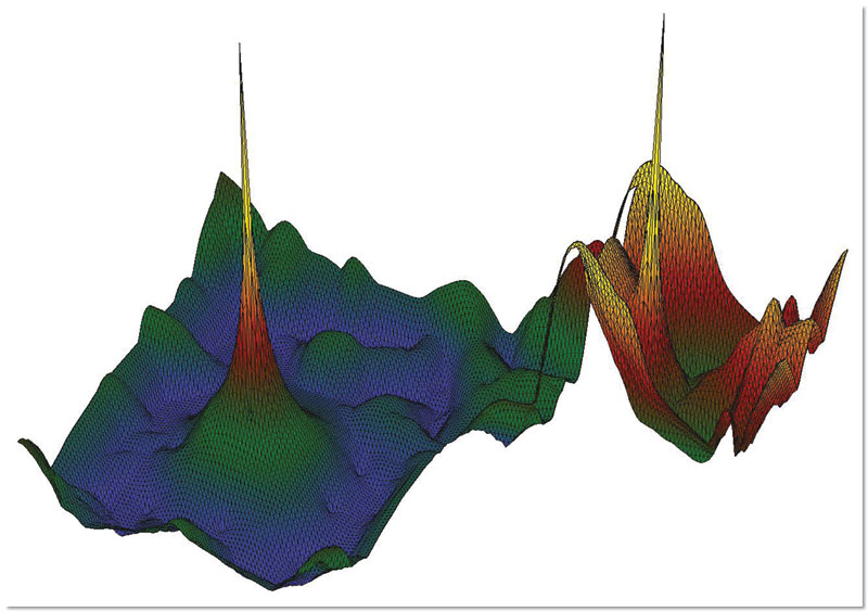
Figure 2
A pre-route noise analysis of a PDN in HyperLynx PI
Two DC issues
For DC, the problem becomes much simpler, but failures can be much more severe. The goal is still to minimize the impedance of the PDN, but the main concern is providing enough metal to distribute potentially tens-of-amps of current. With planes being divided up to accommodate the growing number of different voltages on a PCB, this can be difficult.
An analysis of plane shapes within a PDN can be very useful in identifying areas of low voltage (Figure 3, p. 49). Areas of the board where voltage drops below a certain threshold can lead to IC malfunctions, including SI problems and logic errors.
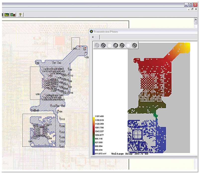
Figure 3
Plot of DC voltage from a power plane analysis
Areas of high current density on the PCB are an equal concern. They can be caused by neck-downs that are the result of partitioning the plane. But they are also common in dense connector and IC pinfields, where antipads eliminate a great deal of the copper on plane layers.
Areas of high current density lead to voltage drop, but can also lead to board failure. A narrow neck-down can act like a fuse that ultimately disconnects power. If the current density is high enough, a neck-down can also lead to dielectric breakdown and even cause the board to catch fire. As such, it is crucial to monitor areas on the planes where current densities may become excessive.
Analysis of the PDN at DC will produce this useful current density information, as shown in the plot in Figure 4. It is also important to monitor current through vias connecting planes together or connecting VRMs to planes. Vias can act as similar neck-downs and areas of high current density, leading to similar failures as those outlined above.
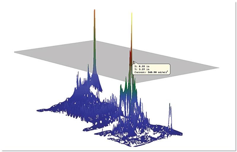
Figure 4
3D plot of current density on a power plane, performed with HyperLynx PI
Mentor Graphics
Corporate Office
8005 SW Boeckman Rd
Wilsonville
OR 97070
USA
T: +1 800 547 3000
W: www.mentor.com

I need to know the allowable current density at FR4 Outer & Inner Layers per 1mm square of Cooper, 1/2 oz & 1.5 oz thickness.
Thanks a lot.
Noah caspi.