Combining yield and performance in behavioral models for analog ICs
The article describes an algorithm that combines performance and variation objectives in a behavioral model for a given analog circuit topology and process. The tradeoffs between performance and yield are analyzed using a multi-objective evolutionary algorithm and Monte Carlo simulation. The results indicate a signi?cant improvement in overall simulation time and ef? ciency compared to conventional simulation-based approaches, without a corresponding drop in accuracy. This approach is particularly useful in the hierarchical design of large and complex circuits where computational overheads are often prohibitive. The behavioral model has been developed in Verilog-A and tested extensively with practical designs using Cadence Design Systems’ Spectre simulator.
Introduction
The last decade has seen increasing integration of analog and digital functional blocks onto the same chip. In such mixed-signal environments, analog circuits must use the same transistors as their digital neighbors. The increasing complexity and accuracy of device models has led to wide acceptance of simulation and optimization design techniques for analog blocks over hand calculations.
With reducing transistor sizes, the impact of process variation on analog design has become very prominent and can lead to circuit performance and yield falling below specification. This issue has led to the consideration of yield in the design process, known as design for yield (DFY).
The use of hierarchical design is commonplace in the IC design world and involves breaking down a large system into its constituent building blocks. Not only does this approach simplify the design task but it also speeds up the design flow by encouraging reuse.
Source: Southampton University
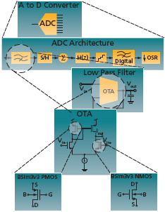
FIGURE 1 A typical system design hierarchy
Behavioral and macro modeling is a useful technique that involves developing models from simulation that relate performance to circuit parameters. Although the initial time investment is high, subsequent design flows are significantly faster.
This paper outlines a novel approach that develops a combined performance and statistical variation behavioral model for analog circuits. Multi-objective optimization (MOO) is used to capture optimal design points, then a statistical variation analysis is performed using Monte Carlo simulation. A behavioral description is constructed to model the performance and variation of the circuit.
Background
Multi-objective optimization
The optimization formulation for more than one objective function is called multi-objective optimization (MOO) and it can be generally stated as:
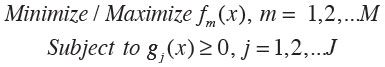
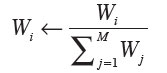
Where fm(x) is the set of M performance functions and gj(x) is the set of J constraints. The outcome from MOO is a set of optimal solutions. MOO has an objective space with the number of dimensions equal to the number of objectives. Figure 2 shows the relationship between the parameter space and objective space where each point in the parameter space is a solution that corresponds to a point in the objective space. The black curve shown on the objective space is called the Pareto front and all solution points lying on this curve are called Pareto-optimal solutions. For example, point B is an example of a non-Pareto optimal point since a more optimal solution exists: point A. The method used in this work combines performance into a single objective using the following weighted summation, where Wm are the weightings for the performance functions:
![]()
Table model functions
Behavioral models employing table model functions require the generation of sampled data points from circuit simulation. Interpolation and extrapolation techniques are then used to estimate a new value from the set of known values. Verilog-A supports three types of spline interpolation: linear, quadratic and cubic. The choice of interpolation is a trade-off between accuracy and complexity. Cubic spline interpolation has been employed in this work to maximize accuracy. The third degree polynomial used to create the piece-wise interpolation curve is defined by the following equation, where ai, bi, ci, and di are the coefficients for the polynomials.
![]()
Source: Southampton University
FIGURE 2 Parameter space and objective space
Source: Southampton University
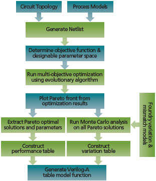
FIGURE 3 Novel yield targeted algorithm
Proposed algorithm
The key steps in the proposed algorithm are shown in Figure 3. These steps are now discussed in more detail.
Netlist and objective function generation
The starting point for the proposed algorithm is made up of a circuit topology, process models and a set of performance functions. The first step involves generating a transistor-level netlist for the chosen circuit topology. From this netlist a set of designable parameters are derived, which will be used to change the circuit’s performance. Examples of designable parameters include a transistor’s length and width. Each parameter will have constraints imposed by the designer, and once determined, these define the parameter space. The performance functions of the circuit are defined as the objective functions, for example, open loop gain or phase margin. Testbench netlists are defined to simulate the performance for a certain set of parameters.
MOO
In this stage, the parameter space is explored and the design improved with respect to the objective functions. The MOO is based on an evolutionary algorithm known as weight-based genetic algorithm (WBGA). It uses a genetic algorithm (GA) to determine the objective function weighting. This is unlike classical weighted optimizations, which often face difficulties in determining the weight vector.
Source: Southampton University

FIGURE 4 Construction of an example GA string
The GA process involves generating several individuals (parameter sets), and optimizing them over multiple generations, using selection techniques to identify the best solutions. The individuals are encapsulated in a set of parameters and weights defined as a GA string. Figure 4 shows an example of the GA string for four designable parameters and two objective function weightings.
P1-P4, W1 and W2 are the designable parameters and performance weights respectively, where the weights for the performance functions are normalized using eq.4, as follows.
During optimization, populations of the GA string individuals are randomly generated. Throughout the evolutionary algorithm, the individuals will go through a process of crossover, mutation and selection from one generation to another. The evolving designable parameter set replaces the existing designable parameters in the netlist. This netlist is then simulated and the performance for each of the objective functions is determined. The performance functions are multiplied by their respective weights given in the GA string and summed to determine a total (normalized) fitness score. This summation is shown in the following equation.
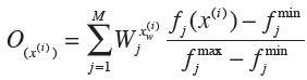
Where fj(x(i)) is the objective function and wjx is its weight. This process will continue until the total number of generations is reached.
Performance model from Pareto front
In a MOO with conflicting objectives, there cannot be a single optimum solution. The previous optimization step results in a number of optimal and non-optimal solutions. It is necessary at this point to determine the Pareto front that consists of the most optimal, non-dominated solutions in the objective space. The two conditions below outline the procedure to establish these non-dominated solutions, thus giving the Pareto front:
a) Any two solutions of the optimal set must be non-dominated with respect to each other.
b) Any solution that does not belong to the optimal set is dominated by at least one member of the optimal set.
Having obtained the Pareto front, the optimal performance functions and their designable parameters are stored in a data file that defines the optimal performance model of the design.
Variation model from Monte Carlo analysis
It is important to consider process variation as early as possible, as it can often reduce the overall yield. This step in the proposed algorithm uses Monte Carlo (MC) analysis to model degradation of the performance function due to process variation. The MC analysis uses foundry variation models to simulate the effect of randomly selected parameter values on a circuit’s performance. During this step in the algorithm, MC analysis is run for each parameter solution set that lies on the Pareto front. From this simulation, a set of performance variations is obtained.
Table model generation
The performance and variation data obtained from the previous stage are used to define the look-up table for a ‘$table_model()’ function in Verilog-A. This function allows the module to approximate the behavior of a system by interpolating between the performance and variations data points extracted from the MC analysis. At this stage, data files exist that describe the performance and variation functions for all the designable parameters. The syntax of the ‘$table_model()’ function is shown below:
$table_model(f1,f2, “datafile.tbl”, “control_string”);
Where ‘f1’ and ‘f2’ are the performance functions, ‘datafile.tbl’ is the text file that contains the performance functions and design parameters, and ‘control_string’ determines the interpolation and extrapolation method. In this algorithm, a cubic spline method is used for the interpolation. No extrapolation method is used, in order to avoid approximation of the data beyond the sampled data points. A ‘$table_model()’ function is created for both the performance functions and the variation functions.
Design example: symmetrical OTA
This section presents a complete design example using a symmetrical operational transconductance amplifier (OTA) as the target circuit. OTAs are fundamental building blocks, often employed in analog circuits such as filters. All the following simulations were performed using the Cadence Spectre simulator with foundry level BSim3v3 transistor models from a standard 0.35um AMS process (C35B4).
Source: Southampton University
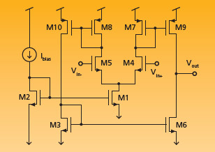
FIGURE 5 Symmetrical OTA topology
OTA design and objective functions
The initial chosen circuit topology is a symmetrical OTA shown in Figure 5. The first step determined the designable parameters for the topology. Here, the lengths and widths for M3 to M10 give eight designable parameters (M1 and M2 dimensions are fixed). The two performance functions for the OTA are the open-loop gain and the phase margin, which both have a weighting.
MOO
The designable parameters, W1-W4 and L1-L4, are constrained within a reasonable range. Table 1 shows these ranges along with the two normalized performance function weights, Wg1 and Wg2.
Once the parameters have been determined, a GA string can be constructed consisting of these and the performance weightings (Figure 6).
Source: Southampton University

FIGURE 6 GA string for the design example
The parameters are all normalized to keep them within the same range of [0~1]. The weighting vectors have already been normalized between [0~1] using eq.4. Each individual generated by the GA will consist of a set of designable parameters as defined by the GA string. The designable parameters are used for simulation, and the weight vectors for the weight summation.
The same testbench netlist was used to determine both the open-loop gain and phase margin for each individual. The total fitness score for each individual was calculated using the normalized weighted-summation formula explained in the previous section. A total of 100 generations each with a population size of 100 were used in this case, giving a total number of samples for the optimization of 10,000.
During the MOO, the GA generates and optimizes the designable parameters and weight vectors to achieve a higher fitness score, and hence optimizes the performance functions. The result is a full set of designable parameters, weight vectors and performance functions.
Source: Southampton University
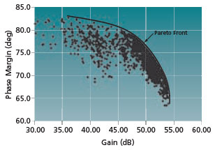
FIGURE 7 Gain and phase margin for individuals
Pareto-optimal front
To illustrate the results of the optimization, Figure 7 shows a plot of open-loop gain and phase margin for the 10,000 individuals in the example. The Pareto front can be clearly seen and contains 1,022 optimum solutions (i.e., circuit candidates). These solutions define the performance model and this information is stored in a data file.
Monte Carlo analysis
Every optimal solution on the Pareto front undergoes a Monte Carlo simulation using process variation and mismatch models. Some 200 samples were chosen for the simulation, and the variation for each performance is calculated from these. This completes the variation model and this information is stored in a data file.
At this point, a combined performance and variation model for the OTA is developed. Selection design points are shown in Table 2, which details the associated performance and variation values for each point. This table is defined as a look-up table for a ‘$table_model()’ function with the resulting Verilog-A model given below:
analogue begin
gain_delta = $table_model (gain, “gain_delta.tbl”, “3E”);
pm_delta = $table_model (pm, “pm_delta.tbl”, “3E”);
gain_prop = ((gain_delta/100)*gain)+gain;
pm_prop = ((pm_delta/100)*pm)+pm;
$display (“Propose Gain : %e”, gain_prop);
$display (“propose PM : %e”, pm_prop);
lp1 = $table_model (gain_prop,pm_prop,”lp1_data.tbl”,”3E,3E”);
lp2 = $table_model (gain_prop,pm_prop,”lp2_data.tbl”,”3E,3E”);
lp3 = $table_model (gain_prop,pm_prop,”lp3_data.tbl”,”3E,3E”);
lp4 = $table_model (gain_prop,pm_prop,”lp4_data.tbl”,”3E,3E”);
fptr=$fopen(“params.dat”);
$fwrite(fptr, “\n Generated Design Parameters\n “);
$fwrite(fptr, “%e %e %e %e”, lp1,lp2,lp3,lp4);
$fclose(fptr);
$display (“params: = %e %e %e %e”, lp1, lp2, lp3, lp4);
gain_in_v = pow(10,gain_prop/20);
V(out) <+ V(inp)*(-gain_in_v)-I(out)*ro;end
From a given performance specification, the model will interpolate a new performance value that can produce the highest yield based on the performance variation. A new set of designable parameters is then interpolated from this new performance value. Table 3 shows an example where the required performance is a gain of greater than 50dB and a phase margin of greater than 74 degrees. The variation for the gain is obtained from the ‘$table_model()’ function. In this case, the relevant look-up table points are those shown in Table 2 where it can be seen that the gain of 50dB is between design points 24 and 25. Interpolation is used to determine the variation for the gain between these points (0.51%). From this variation value it can be seen that the actual gain may vary from 49.75dB to 50.26dB. Therefore, in order to achieve maximum yield, the specified gain of the design must be at least 50.26dB. This will ensure that the required 50dB gain will be achieved within the process extremes. The value of 50.26dB therefore becomes the target performance value, and using this new value, the design parameters are interpolated from the performance table. The same strategy is applied for the phase margin. Both of the new performance values for gain and phase margin will produce 100% yield.
Source: Southampton University
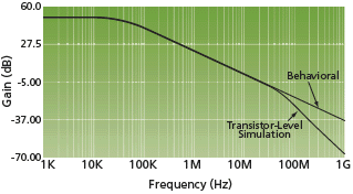
FIGURE 8 Open loop gain comparison
To verify the performance and yield from the behavioral model design, a comparison has been made with transistor-level simulation using design parameters obtained from the ‘$table_model()’. This comparison is shown in Table 4. The percentage error in passband gain and phase margin was calculated between the OTA transistor simulation and interpolated values. Figure 8 shows the open-loop gain for the Verilog-A model and transistor model. It can be seen from these comparisons that the Verilog-A function matches closely with the transistor-level simulation.
Figure 8 shows a divergence in the comparison above 40MHz, attributed to parasitic poles in the transistor circuit. Although these higher order effects are not modeled in this example, they could easily be incorporated if required. A Monte Carlo simulation using 500 samples was carried out and verified a yield of 100%.
Table 5 summarizes the parameters associated with model development. A total of 10,000 simulations were run in the initial MOO step for the performance model, and Monte Carlo analysis was performed on 1022 Pareto optimal points for the variation model. The OTA design optimization stage took four hours on a 1.2GHz Ultra Sparc 3, which compares well with a previously reported optimization time of seven hours for the same circuit.
Conclusions
This paper has presented a new algorithm that combines performance and process variation objectives in a behavioral model for an analog circuit topology. MOO with genetic algorithm is used to explore trade-offs between performance and yield, leading to a set of Pareto optimal solutions for the design. Monte Carlo variation analysis is performed on all the Pareto optimal solutions, and a table is constructed for both the performance and variation analysis. A behavioral model developed in Verilog-A is used together with this table to determine the parameters required to achieve the highest yield within a given specification. After the initial time investment to create the model and table, there are significant improvements in overall simulation time and efficiency compared to conventional simulation-based approaches. These benefits are enjoyed without a corresponding drop in accuracy.
Source: Southampton University
|
Design Parameter: |
Range: |
|---|---|
|
W1 (M5,M4) |
10um – 60um |
|
L1 (M5,M4) |
0.35?m – 4?m |
|
W2 (M7,M9) |
10um – 60um |
|
L2 (M7,M9) |
0.35?m – 4?m |
|
W3 (M10,M8) |
10um – 60um |
|
L3 (M10,M8) |
0.35?m – 4?m |
|
W4 (M3,M6) |
10um – 60um |
|
L4 (M3,M6) |
0.35?m – 4?m |
|
Wg1 (Gain weight) |
0 – 1 (normalized) |
|
Wg2 (Phase weight) |
0 – 1 (normalized) |
TABLE 1 Design parameters.
Source: Southampton University
|
Design: |
Gain (dB): |
?Gain (%): |
PM (deg): |
?PM (%): |
|---|---|---|---|---|
|
21 |
49.78 |
0.52 |
76.3 |
1.50 |
|
22 |
49.90 |
0.52 |
76.1 |
1.51 |
|
24 |
49.98 |
0.51 |
76.0 |
1.51 |
|
25 |
50.17 |
0.51 |
75.8 |
1.52 |
|
26 |
50.35 |
0.50 |
75.5 |
1.56 |
|
27 |
50.45 |
0.49 |
75.3 |
1.57 |
|
34 |
51.06 |
0.44 |
74.1 |
1.69 |
|
35 |
51.14 |
0.51 |
74.0 |
1.71 |
|
37 |
51.24 |
0.42 |
73.8 |
1.69 |
|
38 |
51.62 |
0.42 |
73.2 |
1.68 |
TABLE 2 Performance and variation values
Source: Southampton University
|
Performance: |
Required Performance: |
Variation: |
New Performance: |
|---|---|---|---|
|
Gain |
> 50dB |
0.51% |
50.26dB |
|
Phase Margin |
> 74 deg |
1.71% |
75.27 deg |
TABLE 3 Interpolation example
Source: Southampton University
|
Performance Functions |
Transistor Model |
Verilog-A Model |
% error |
|---|---|---|---|
|
Gain |
50.73 |
50.26 |
0.93% |
|
Phase Margin |
76.06 |
75.27 |
1.03% |
TABLE 4 Performance comparison
Source: Southampton University
|
Parameters: |
Values: |
|---|---|
|
No. Generations |
100 |
|
Evaluation Samples |
10,000 |
|
Pareto Points |
1022 |
|
CPU Time (1.2GHz Sparc 3) |
4 hours |
TABLE 5 Design parameter summary
Electronic Systems & Devices Group
School of Electronics and Computer Science
University of Southampton
Southampton
SO17 1BJ
United Kingdom
T: +44 (0)23 8059 6000
