Tackling the design challenges of PCIe 5.0
Moving up to PCIe 5.0 speeds demands rethinking everything from silicon design through choice of PCB material and connectors up to track layout and validation.
PCI Express (PCIe) is a well-established interface used in computing and networking applications, which continues to evolve to meet demands for higher data rates and greater bandwidth. The PCI-SIG industry consortium has responded to this trend by announcing its latest specification, PCIe 5.0, which raises the standard’s data rate to 32GTransfer/s, and doubles the link bandwidth from 64Gbyte/s to 128Gbyte/s. Figure 1 shows the evolution of PCIe interconnect and total bandwidths.
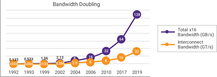
Figure 1 PCI-SIG bandwidth growth (Source: Synopsys)
Challenges for system designers
PCB traces, connectors, cables, and even IC packages all limit system bandwidth and make high data-rate designs a challenge. The high signal frequencies increase copper loss and power loss, which limits transmission distances. The channel losses at higher signal frequencies also cause signal integrity (SI) issues.
There are many types of PCIe channel, from connectorless chip-to-chip topologies through to complex server topologies with backplanes, multiple PCB cards and multiple connectors. Figures 2 through 5 show that most PCIe channels have an IC package at each end and multiple PCBs, for example a processor board, add-in card, and riser, all connected with mezzanine or PCIe card electromechanical (CEM) connectors.
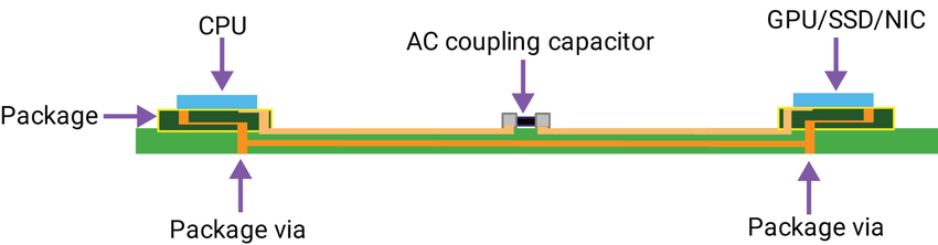
Figure 2 Chip-to-chip interface, the simplest channel with no connector (Source: Synopsys)
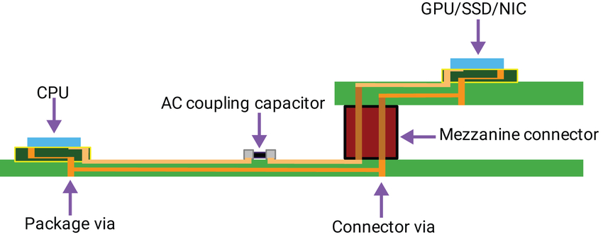
Figure 3a Channel with one mezzanine connector (Source: Synopsys)
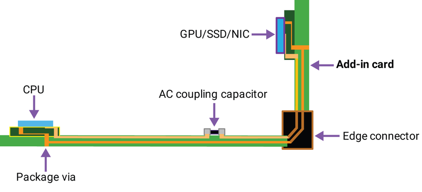
Figure 3b Channel with an edge connector (add-in card) (Source: Synopsys)
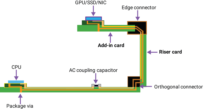
Figure 4a Channel with two connectors using a riser card and an add-in card (Source: Synopsys)
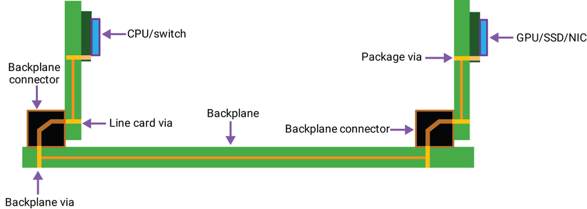
Figure 4b Standard backplane channel with two line cards and two connectors (Source: Synopsys)
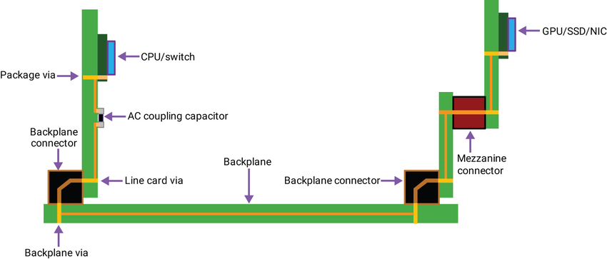
Figure 5 Complex backplane channel with more than two connectors (Source: Synopsys)
PCIe system designers have used generic FR4 PCB materials and wirebond packaging for most applications up to 8GTransfer/s rates. At 32Gtransfer/s, this is no longer possible. Designers are now moving to lower-loss materials such as MEGTRON to counter increasing channel loss, even at the 16GTransfer/s maximum speed of PCIe 4.0.
PCBs may also be designed with wider spaces between traces to improve system-level SI. Many designs will also use enhanced CEM connectors or custom mezzanine connectors, and will back-drill the PCB vias to minimize stub lengths. In a few cases with very long channels, re-timers may also be used.
All these enhancements come at a cost. MEGTRON can cost 1.2 to 2.5 times more than FR4, and PCB traces may need to be further apart to improve jitter performance, resulting in a larger and more expensive PCB. Back drilling the via stubs, part of the board-making process, also adds cost. The use of enhanced or custom surface-mount connectors drives up costs when compared to through-hole CEM connectors. And the use of re-timers takes up board area, driving up board and assembly costs, increasing the bill of materials, and boosting data-path latency and system power.
To validate their designs, system designers must work with SI engineers, package designers, SoC designers, and PCB designers to model each component in their channel to verify its end-to-end performance.
The challenge of designing PCIe 5.0 PHYs
You can’t build 32GTransfer/s PHYs to meet the requirements of PCIe 5.0 by making incremental improvements to a 16GTransfer/s PHY. The transmitter and receiver equalisation circuits need significant improvements to counter the increase in channel loss at 32GTransfer/s. Many sub-circuits also need redesigning to meet the tighter jitter parameters, jitter limits, and return-loss requirements at all process, voltage, and temperature corners.
The PHY for PCIe 5.0 is also expected to support features such as lane margining via the controller, and the Separate Reference Clock Independent Spread Spectrum Clocking strategy. Such enhancements and additional constraints make designing a PCIe 5.0 32GTransfer/s PHY extremely complex, requiring competencies in many areas to achieve a low-power, small-area, and low-latency PHY with optimal signal and power integrity.
A silicon-proven PHY with accurate models enables designers to model, design, and simulate an end-to-end channel to optimize and validate their system design. Synopsys is already developing PCIe 5.0 IP, using its decades of experience in implementing PCIe in multiple processes, and SoC designers can work with the company to discuss PCIe channel performance needs at higher data rates, as well as IP integration, timing closure, SI, packaging, and manufacturing needs.
Further information
PCIe 5.0 IP demonstration video
DesignWare IP Solutions for PCI Express
Author
Rita Horner is a senior technical marketing manager at Synopsys.
