Catch multi-patterning errors clearly at advanced nodes
How to address increasingly complex patterning issues and debug them efficiently as design moves toward 12 and 10nm.
When double patterning (DP) was introduced for 20nm processes, the DP layers had relatively simple and straightforward constraints on the spacing between the two exposures. These constraints were captured in design rules and expressed to the DP engine through opposite mask requirements. But DP layer rules are getting more complex for smaller nodes, with some layers requiring triple or quadruple patterning, and even DP layers are encountering fundamental new constraints.
DP verification tools have evolved to keep pace but detecting multi-patterning errors is only one piece of the solution verification engineers need. They also need a powerful debug capability driven by well-designed visualization to make sense of the complexity of multi-patterning verification errors at advanced nodes.
Consider the following DP constraint changes in advanced nodes: opposite-mask spacing; forbidden pitches; and double-spaced lines.
Opposite-mask spacing
The first big change is opposite-mask spacing. This expands the idea of minimum same-mask spacing to minimum opposite-mask spacing. At 20, 16 and 14nm, the minimum opposite-mask spacing requirements, combined with the minimum polygon width requirements, create a pitch in which the second-neighbor shape is always more than the minimum same-mask distance away (Figure 1).
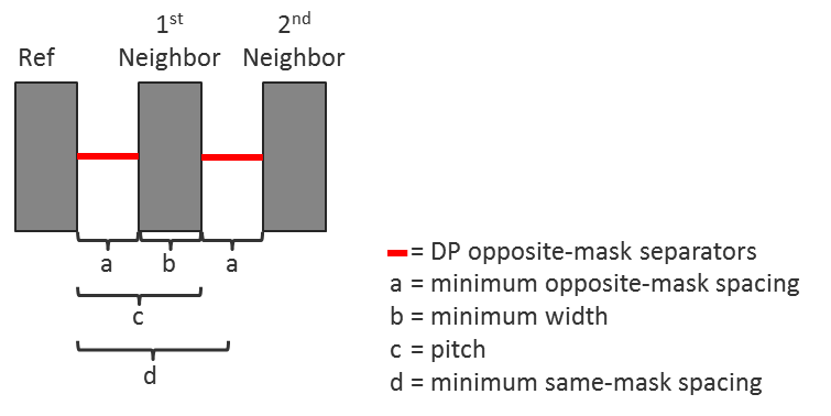
Figure 1: Typical pitch relationships and constraints in 20/16/14 nm double patterning layers (Mentor)
However, in some process layers (beginning at 12nm), you can meet the minimum opposite-mask spacing and minimum width, but the second-neighbor shape can still be closer than the minimum same-mask spacing from the reference shape. Because of this, it is possible to have an opposite-mask separator constraint spacing requirement between the reference and second-neighbor shapes (Figure 2).
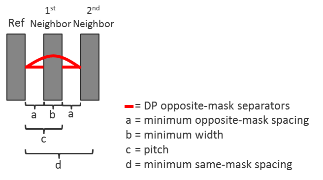
Figure 2. New pitch relationships and constraints in double patterning layers at 12nm and below (Mentor)
Forbidden pitches
Another new spacing constraint at advanced nodes involves constructive and destructive interference patterns that can create specific spacings that are not reliably printable. These spacings, known as forbidden pitches, typically appear as a specific spacing or range of spacings that prohibit the two involved polygons from being on the same mask, even if they are more than the minimum same-mask distance from each other (Figure 3).
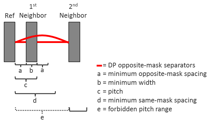
Figure 3. Forbidden pitch relationships and constraints (Mentor)
Double-spaced lines
With self-aligned double patterning (SADP) techniques, allowed pitches are even more restricted, because the spaces are defined by the sidewalls [2]. Designers can create some variation in pitch by placing two mandrel shapes exactly two sidewall widths apart. The two sidewalls will merge to form a single dielectric space between them (Figure 4). For this double-spaced line to manufacture properly, both polygons must be the same color. Communicating this requirement to the coloring engine requires a same-mask separator that, unlike the traditional opposite-mask separator, tells the coloring engine that the two shapes must be on the same mask.
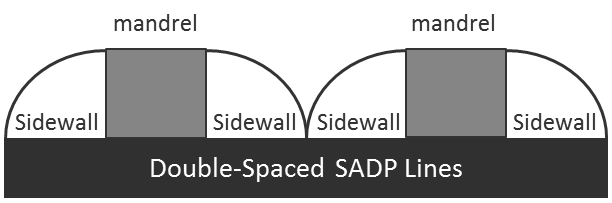
Figure 4: Double-spaced lines in SADP (Mentor)
Double patterning error detection
These new constraints have a big effect on double patterning error detection and visualization. Before, DP errors were based on the physical view of the data, in which the polygons and separators form a connected ring with a ‘hole’ in the middle. Any odd polygon count around this hole formed an error cycle, so visualization was accomplished by drawing a thin polygon line around the inner edges of the hole (Figure 5).
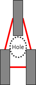
Figure 5. Traditional odd-cycle ‘hole’ error ring (Mentor)
Because opposite-mask separators can now extend across the first-neighbor to the second-neighbor shape, it is possible to have an odd cycle of separator constraints based on three polygons in a row, and real DP errors can be missed because there is no ‘hole’. In other words, the cycle configuration in the physical space is no longer planar (Figure 6).
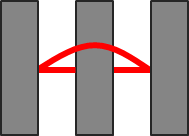
Figure 6. “No-hole” non-planar odd-cycle DP constraint (Mentor)
Those forbidden pitch constraints present another challenge to physical-based DP error detection methods. The nearest neighbor to a polygon may be far enough away to allow same mask coloring, but the second-neighbor shape may be located in a forbidden-pitch range and require color alternation. The separator communicating the color alternation requirement between the reference and second neighbor must cross the first neighbor in planar space. Because separators can now physically cross over polygons that are not involved in the error, it can appear as though those polygons are part of the error when they are not. Simply counting all the polygons ‘touching’ separators in an error ring can produce a false or missed error, depending on the situation, as shown in Figure 7.
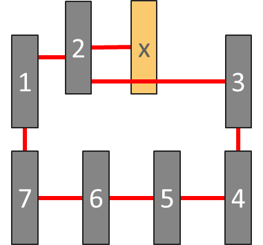
Figure 7. Double patterning layout with non-involved polygons (Mentor)
In this layout configuration, the cycle configuration in the physical space is no longer planar. Polygon ‘x’ and polygon ‘2’ require color alternation between them, as do polygon ‘2’ and polygon ‘3’. Color alternation is not required between polygon ‘x’ and polygon ‘3’, but the separator between polygon ‘2’ and polygon ‘3’ crosses polygon ‘x’. If polygon ‘x’ is included in the count, this configuration would be considered an even cycle of eight, when it is actually an odd cycle of seven, leading to a missed error.
Designers may encounter similar situations with anchor-path violations (Figure 8). The color alternation requirements for this path are not compatible with the anchored shapes on each end. However, if polygon ‘x’ is mistakenly considered to be in the path sequence, the configuration would falsely be considered legally colorable.
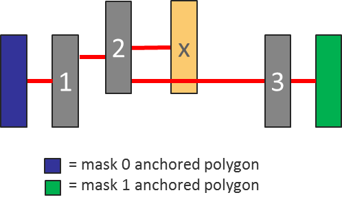
Figure 8. Anchor-path violation with non-involved polygons (Mentor)
Lastly, in the presence of both same- and opposite-mask separators, polygon count is no longer sufficient to determine an error, as shown in Figure 9. The first configuration appears to be an odd-cycle error, as there are three polygons involved. However, because the same-mask separator between the two bottom polygons requires them to be the same color, this configuration can actually be legally colored with two colors, and is not an error. The second configuration appears to be a legal even cycle. However, the same-mask separator requiring the same color for both of the bottom polygons makes this configuration not legally colorable with two colors, and therefore is actually an error.
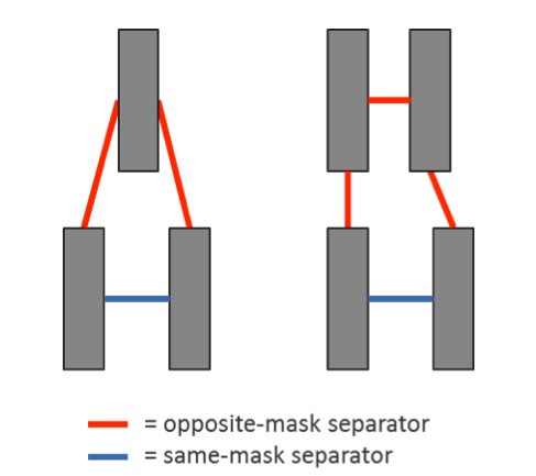
Figure 9. Layout configurations with opposite-mask and same-mask separators (Mentor)
The solution? Abandon error detection via polygon count in a planar physical arrangement. Instead, the cycles are analyzed in their virtual graph representation, and validity is based on color parity rather than node count.
Figure 10 shows a cycle of four polygons with a same-mask edge at the bottom. In a count-based approach, you simply count polygons from 1 to 4 to find this is an even cycle, which is presumed to be legal. For the color-parity-based approach, you use a virtual graph, starting at one of the nodes (in this case, the upper left node). This node starts with a parity of 0, and the parity changes as the cycle is traversed. As you move counter-clockwise to the bottom-left node, the parity changes to 1 because of the opposite-mask edge. As you move to the bottom-right node, the parity remains 1 because you have a same-mask edge. Moving to the upper-right node, parity flips back to 0 because of the opposite-mask edge. Finally, you move back to the upper-left node and flip the parity again to a 1, because of the opposite-mask edge. Since the parity on that node must be both a 1 and a 0, you have found an error.
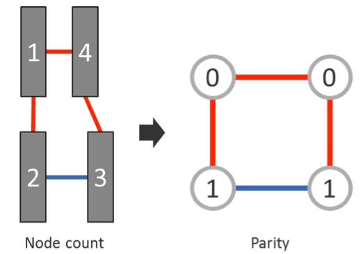
Figure 10. Polygon count vs. parity analysis for DP error detection (Mentor)
Double patterning error debugging
While detecting valid double patterning errors is the first challenge at advanced nodes, it is useless unless the designer can understand and resolve the problems. Traditional error-ring and anchor-path visualization markers do not effectively annotate and explain these types of errors. There are three primary issues in advanced error visualization:
- Identifying which polygons are and are not involved in the error.
- Effectively mapping a non-planar ring or path onto a planar layout.
- Describing a cycle error with no ‘hole’ area on the planar layout.
Advanced DP toolsets have added new ways to visualize these new rule violations. For example, there is the enhanced error ring visualization in the Calibre Multi-Patterning functionality, part of the Mentor physical verification suite. It widens the ring to show where it interacts with a polygon, enabling you to see that only seven of the eight polygons actively participate in the cycle—thus it is a real error (Figure 11).
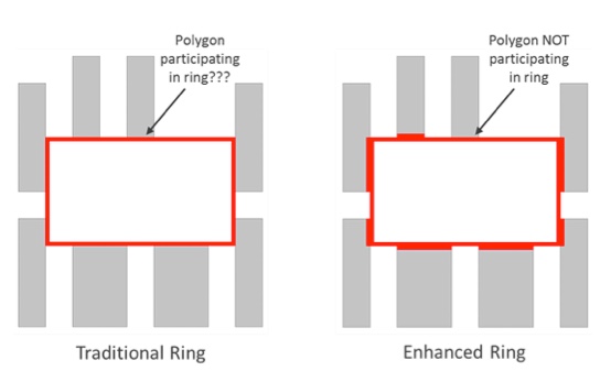
Figure 11. Traditional vs enhanced error ring visualization with a non-participating polygon (Mentor)
Similarly, widening the path through the involved polygons in an anchor-path makes it obvious that the wide polygon to the right of center is not actually involved in the path (Figure 12).
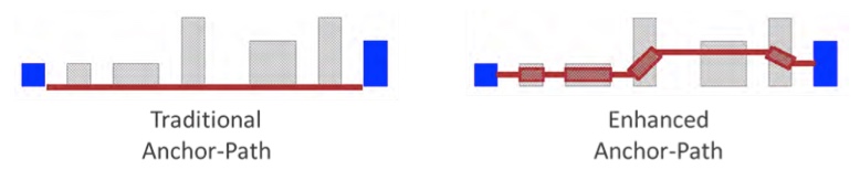
Figure 12. Traditional vs enhanced anchor-path error with a non-participating polygon (Mentor)
In Figure 13, the polygons and separators form a virtual ‘figure 8’ odd-cycle on the planar layout. Using the traditional ‘donut hole’ of an odd cycle only marks the smaller of the two ‘figure 8’ holes, leaving the designer unsure where the error occurs. With enhanced error visualization, the entire ‘figure 8; is annotated, including the twist in the middle where the interactions cross each other. Now the designer knows which polygons are involved, and what might actually be causing the error.
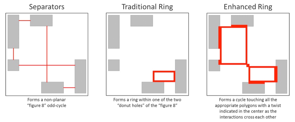
Figure 13. Enhanced error visualization of a non-planar odd-cycle (Mentor)
In addition to visualization improvements, there have been new opportunities to improve error debug efficiency. One goal is to quickly focus the designer’s effort on the most fundamental error that occurs in a particular location. Many DP errors can cause other, more complex DP errors to occur. Showing all of these to a designer may distract from the root problem, and result in unnecessary designer time or design area being spent on fixing a particular issue.
Enabling DP verification tools to filter out complex errors and partition them into more focused and specific categories helps designers focus on the root cause. Applying this filtering intelligently ensures that a given design issue only produces output for the most specific and concise error type, even when it causes multiple types of errors. The result is to narrow the focus of debug and remove noise in the output.
Combining this new partitioned and filtered DP error visualization with new in-design DRC checking tools also lets designers quickly test multiple possible solutions to find the optimum solution, greatly enhancing DP debug and error fixing productivity while also improving design quality and manufacturability.
As DP requirements have evolved and become more complex, so has DP verification functionality. Advanced DP tools can not only identify the most complicated DP errors at advanced nodes, but also are better at helping the designer understand and fix DP issues quickly and with clarity.
About the authors
Alex Pearson is a Calibre Technical Marketing Engineer in the Design to Silicon division of Mentor, a Siemens business, currently focused on multi-patterning techniques for physical verification at advanced process nodes. He received his B.Sc. in Electrical and Computer Engineering from Oregon State University, and is completing a master’s degree in the same field at Portland State University. Alex can be reached at alexUNDERSCOREpearsonATmentorDOTcom.
David Abercrombie is the Program Manager for Advanced Physical Verification Methodology at Mentor, a Siemens business. Prior to joining Mentor, David managed yield enhancement programs in semiconductor manufacturing at LSI Logic, Motorola, Harris, and General Electric. David received his BSEE from Clemson University, and his MSEE from North Carolina State University. He may be reached at davidUNDERSCOREabercrombieATmentorDOTcom.
