Balancing devices and manufacturing
Fab owners are looking to bring down their energy consumption to match the greening of semiconductors themselves.
The electronics industry has a strange, often tense relationship with the worlds of energy efficiency and all things ‘green’. It wants to be seen as a great enabler of cutting carbon emissions and better husbandry of the world’s resources. It has some justification in this regard.
Semiconductor companies are extending the battery life and functionality of all manner of mobile devices, and their most powerful processors are today designed to specifically reduce the massive amounts of energy needed simply to cool today’s ubiquitous server farms.
Then there is electronics’ role in driving down the cost of solar energy, specifically by bringing Moore’s Law to bear on photovoltaic technology and pushing it toward the crude acquisition cost target of $1 per watt (today’s purchase price stands at around $4.50).
However, there is then the question of manufacturing. At this year’s International Solid State Circuits Conference (ISSCC), Dr. Oh-Hyun Kwon, president of Samsung’s semiconductor operations, noted that chipmakers’ fabs still use 40TWh of energy every year, more than the state of Michigan with a population of 10 million people.
“The [power] consumption in 2008 was 47 percent more than that of 2001 and demonstrates a 7 percent annual growth rate for the last two years,” he said. During the latter period, manufacturing processes were ramping up toward—and remain very much in the roll-out of—the latest process shrink, this time to the 28/32nm node.
Over the course of 2011, the industry is continuing to invest heavily in fab capacity, so much so that analysts at Gartner recently warned that it could be headed for an oversupply in spite of the disruption caused by the earthquake in Japan. SEMI, the trade association for the chip manufacturing chain, confirmed the spending spree in its most recent forecast.
“Total spending on fab projects could approach $47.2B this year, above the estimated $38.6B spent in 2010,” said Christian Gregor Dieseldorff, senior analyst in its Industry Research and Statistics group.
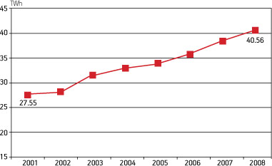
Figure 1
Electric power consumption by the semiconductor industry Source: WSC
According to Dr. Kwon’s model, more money and more fabs imply still more energy consumption. However, this is only part of the story. “Most spending is directed toward upgrading existing facilities,” Dieseldorff continued.
A primary driver here is that fab owners do want to avoid oversupply. The trend away from chip companies producing their own silicon to using third-party foundries has made those foundries much more sensitive to risks when their fabs are not operating at close to capacity. So incremental projects are, for now, more attractive than spending billions on greenfield factories.
However, energy costs are also playing a role in these capex plans. While saving the planet is a desirable goal, saving money spent with utilities has become an equally compelling one.
In April, Intel secured some green kudos with the announcement that it had received a Leadership in Energy and Environmental Design (LEED) ‘silver’ certification under the U.S. Green Building Council-administered scheme for its Ocotillo operations in Chandler, Arizona.
The award is significant because it was granted to an existing rather than a brand new facility—it is a demonstration of what the semiconductor industry can do already. As well as offices and support, Ocotillo houses three generations of fab.
Specific steps taken to ‘green’ Ocotillo included the location of 200kW and 300kW solar arrays in a former parking lot; the build-out of infrastructure to recycle 90 percent of solid waste (more than 10,000 tons) and achieve 66 percent site-wide water conservation (saving 19 million liters of fresh water per day); and the installation of a system to capture all storm water for use on site.
“The Ocotillo campus also utilizes a pipe that feeds water not suitable for drinking from the City of Chandler’s waste water treatment plant directly back to Intel,” said Brian Krzanich, senior vice president and general manager of Manufacturing and Supply Chain for Intel. “As a result, 100 percent of the irrigation water and 95 percent of the cooling tower water is non-potable.”

Intel built its Haifa site specifically to meet LEED green building requirements
Intel’s LEED certification in Arizona is no one-off. In 2010, the company also received awards for sites in Haifa, Israel and Kulim, Malaysia. Nor is it alone in its enthusiasm for that program. TSMC also has LEED awards—as well as recognition under Taiwan’s Ecology, Energy Saving, Waste Reduction and Health scheme—for two of its newer factories: Fab 14/Phase 3 and Fab 12/Phase 4.
This work is largely being undertaken because it also saves money. “We take these steps not just in Arizona, but at our other facilities around the world, because we see a combination of economic advantages and opportunities to reduce our environmental impact, which in turn betters our business,” said Krzanich.
According to metrics developed by the Semiconductor Industry Association, Ocotillo uses 26 percent less energy than a standard chip manufacturing site.
Beyond Intel, TSMC and Samsung, one of the other clear signs that this LEED creed is being more widely adopted comes from International Sematech, the manufacturing think-tank that serves all fab owners.
In June 2009, it set up an Environmental Safety and Health (ESH) division within its ISMI manufacturing initiative. A relatively small-staffed project initially, it promotes technologies and strategies that will help companies to reduce power consumption. Some of these involve large scale renewable installations and recycling, but it also backs transitions to LED lighting and more efficient heating, ventilating, and air-conditioning systems.
Others seek to develop key performance indicators, and ISMI-ESH launched TEECalcII last November, a software tool that tracks the total energy performance of fab equipment (the software is available for public download from www.teecalc.com).
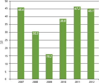
Figure 2
Total worldwide fab spending Source: SEMI
ISMI-ESH estimates that such upgrades can cut utility bills by between 10 and 20 percent, and it is adding techniques to its existing standards arsenal that address, for example, the idle mode consumption of vacuum pumps and point-of-use abatement systems used in chip manufacturing.
At ISSCC, Samsung’s Dr. Kwon noted that many of the machines in a fab still consume 73 percent of full operational energy in standby mode. Cutting this to just 50 percent could save 2.3TWh of power across the whole sector every year. Those savings alone could represent a 6 percent cut in energy use.
However, his speech also began to look toward another impending challenge for chipmakers. Although companies have begun to take steps to control the existing infrastructure, overall power consumption continues to rise. This is where innovation becomes ‘the enemy’.
It is becoming ever more expensive to build fabs. GlobalFoundries has estimated that a state-of-the-art factory today costs a minimum of $4B to build. The implications for ROI are obvious, and there is a shift on the horizon that is set to lift that price tag even higher.
Today’s advanced fabs produce chips on 300mm wafers. Increasing wafer size while reducing device dimensions and device size equals still greater profitability, but at the outset, it is a big bet and after that the consequences are considerable. Toshiba, the world’s third largest chipmaker, estimates that the last increase in wafer size recast the balance in terms of power consumption.
At fabs running 200mm wafers, 53 percent of energy use was accounted for by the fab facility and 47 percent by the manufacturing equipment within it. At 300mm, that changed to 46 percent consumption for the facility and 54 percent for the equipment. Now, silicon is getting ready to shift from 300mm to 450mm. The first fabs capable of taking the new size going into construction today and actual production runs are due in two years’ time, according to SEMI.
“SEMI’s World Fab Forecast data identifies seven facilities (R&Ds, pilots and volume fabs) in the near future that are candidates for 450mm readiness,” said Dieseldorff. “The first facilities are expected to come on line in 2013, though it remains to be seen if enough mature 450mm tools will be available to fully equip a high-volume fab.” (our italics)
This provides an important context for Dr. Kwon putting energy consumption back on the agenda even though his industry is already working to manage everything that goes around the plant that makes the chips themselves.
“The semiconductor industry is reviewing the main causes of energy inefficiency in manufacturing equipment and processes. Controlling excessive operating margins in equipment and utility systems, along with the development of the next-generation process, can lead to a more energy-efficient manufacturing flow,” he said, but immediately noted that more work is necessary.
“We propose ‘Interdisciplinary Collaboration’ to capture all the possible energy-saving opportunities in the areas relevant to the semiconductor industry. Interdisciplinary Collaboration in this context refers to broad cooperation, not only within the semiconductor industry, but also with the other relevant industries including software, system, and infrastructure. We can further expand the scope of collaboration to academia and industry level consortiums such as WSC (the World Semiconductor Council) and ISMI. We believe all these eco-friendly Interdisciplinary Collaboration efforts will initiate and accelerate industry-wide energy-saving activities, and can make a tremendous contribution toward the relief of the current environmental crisis.”
One caveat needs stating about the move to 450mm: only a handful of companies are likely to adopt the new size, given that it will best suit chips that are made in massive volumes and which are each likely to cost more than $100M to design. Nevertheless, the obvious candidates—Intel, Samsung (particularly as the world’s largest manufacturer of memories) and the two leading foundry groups—will account for an increasingly large proportion of overall output.
However it is sliced, though, the broad collaboration envisaged by Dr. Kwon will be essential. The challenge is balancing the extraordinary technological demands imposed by continuing on a Moore’s Law-like path in a timely way with equipment that can deliver the innovations necessary on tighter power budgets. That conundrum is still some way from being resolved, although the willingness to do something about it is there.
