Automating the SSN verification challenge
Simultaneous Switching Noise (SSN) is the voltage fluctuation caused by the simultaneous switching of groups of output chip I/O drivers that drive high slew rate signals. It has an impact on I/O and core power supply lines and on signal lines, and is an increasingly important challenge for designs that incorporate high performance interfaces, such as DDR.
Power supply line issues include dynamic voltage drop at the core and at the I/O power/ground pins of output buffers. This voltage drop can lead to excessive jitter on critically-timed signals. Signal line issues include timing performance problems and large glitches that cause false state changes in components along the signal line.
To date, lengthy and laborious manual verification methodologies, largely dependent on SPICE, have been needed to address SSN. The author argues, however, that by applying and extending techniques already available in EDA tools, the work can be effectively automated, speeding up design cycles and allowing more time for high-level design analysis.
The increasing use of high performance I/O interfaces forces chip designers to analyze the impact of simultaneously switching output pins that drive high slew rate signals. Signals in DDR interfaces have such a slew rate. Moreover, many bits can switch simultaneously; the timing window specification for data bits is tight (2.5ns for DDR2-400, 1.875ns for DDR2-533); and the valid timing window for data transfer is even tighter (1ns or lower) when SDRAM setup and hold times are subtracted from these numbers.
Simultaneous switching noise (SSN) affects the timing performance of output drivers as well as other I/O and core instances nearby. It can cause large enough glitches on the output signal to falsely switch the state of the next component on the signal path. Additionally, mutual inductance between supply and signal lines along the package and board causes crosstalk, increasing the risk of signal degradation. Susceptibility to voltage fluctuations increases as the operating voltage is reduced. And, with the trend towards more pins on smaller die, the number of pins in close proximity increases, raising the probability of simultaneous switching within an I/O region.
No design cycle is complete until it has verified SSN’s impact on the integrity of on-chip power and of signals driven out of the chip along the package and PCB. Decisions regarding package choice, output signal slew rate, pin sizing, pin placement, and decoupling capacitance placement need to be made based on trade-offs informed by quantitative analysis.
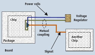
Figure 1. A cartoon view of the main players in SSN
Today, engineers need to manually set up many files for merciless SPICE runs. The process is lengthy and errorprone. This limits the number of experiments that can be performed by designers who would rather spend time on higher-level direction of the simulation, higher-level analysis of the results, and a thorough analysis of trade-offs. Instead, they must dedicate valuable time to ensuring that each pin of each instance in, say, a 50-pin I/O cell has been properly sensitized using V SPICE statements, and the correct voltage entered in the manually-created netlist.
Furthermore, a manual approach limits engineers to using estimated models for on-chip parasitics in the I/O region and surrounding area. They would rather pick an I/O region, and have the setup and simulation done automatically, freeing up time for inspecting the resulting waveforms and experiments in other regions.
What is SSN?
SSN is the voltage fluctuation caused by the simultaneous switching of groups of output chip I/O drivers that drive high slew rate signals. It has an impact on I/O and core power supply lines, and on signal lines.
Power supply line problems manifest themselves as dynamic voltage drop at the core and at the I/O power/ground pins of output buffers. They can also occur at the power/ground pins of nearby core and I/O instances that share the same power grid. This voltage drop can lead to excessive jitter on critically-timed signals. This is particularly an issue for DDR interfaces.
Signal line problems manifest themselves as timing performance problems or, in extreme cases, as large glitches that cause false state changes in components along the signal line. If such a glitch appears on a clock line, registers trigger inappropriately thereby latching incorrect data.
SSN is caused by a combination of package characteristics (large self inductance and mutual inductance) and the rate of change in the current consumption of output drivers, by means of voltage fluctuations on power supply lines and crosstalk between supply-to-supply and supply-to-signal lines inside the package. Figure 1 shows key players in SSN. The output driver is driving a signal line through the package and board. The signal line is affected by mutual inductance (K) to the nearby power supply line driven by the on-board voltage regulator. The high inductance (L) of the power distribution network at the board and package levels combines with the high rate of change of current consumption (di/dt) of the output driver to cause Ldi/dt fluctuations. This degrades the signal line (and nearby instances connected to the same power grid).
The impact of di/dt
Buffers used in the output pins of chips are large and consume large current (i) because they drive large off-chip loads. If they drive signals that have a high slew rate (dv/dt), they need to make the voltage swing (dv) in a small time duration (dt). Thus, they impose a high di/dt on the power grid they connect to. If many such buffers are close to one other and switch simultaneously, their individual di/dt adds up, cumulatively causing large Ldi/dt fluctuations on the power grid.
The following figures and equations explain the contributors of Ldi/dt noise in more detail.
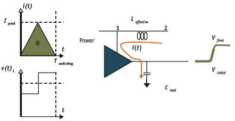
Figure 2. A simplified view of a driver switching to change the signal logic level from 0 to 1. Switching current i charges C loadby charge Qto raise the signal voltage.
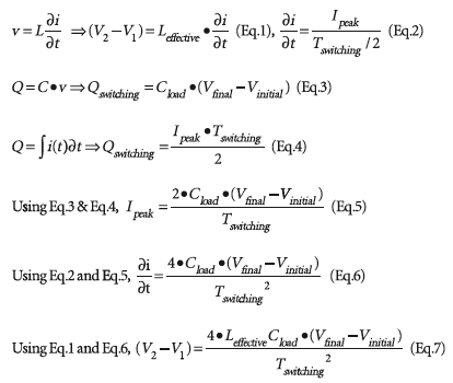
Figure 3. Derivation of contributors to Ldi/dt noise
In Figure 2, the current waveform has been represented with a triangle. Current is zero before and after switching. In Figure 3, (p.28) Eq.2 represents the slope of the triangle in the first half of switching duration. Eq.3 represents the amount of charge necessary to fill the load capacitor for it to charge up from initial voltage level to the final voltage level. Eq.4 represents the amount of charge supplied by the current, and is equal to the area under the curve.
From Eq.3 and Eq.4, the peak current has been brought out, and substituted at Eq.2 to eventually reach Eq.7, which shows the components that affect the voltage drop between node 1 and 2. In the second half of the switching, the voltage drop has a negative sign (i.e., it is a bounce) since the slope of the triangle, hence Eq.2, would be negative.
The importance of slew rate on SSN can be seen at Eq.7. Note that since initial and final voltage levels are fixed for a design, a change in slew rate essentially means a change in switching time. Eq.7 shows that the noise is inversely proportional to the square of switching time, which means that n times shorter duration results in n*n more noise. This square relationship makes the switching time the most important term in the equation, and it is the reason why the slew rate plays such an important role for SSN.
SSN analysis and methodology
Designs with combinations of the following characteristics require SSN analysis:
1. The design has high performance interfaces.
Such interfaces have tighter timing windows, and hence are more susceptible to noise. They also typically have slew rates that cause high di/dt.
2. The design has many output pins switching simultaneously in a neighborhood.
This causes high di/dt localized in a region.
3. The design will be placed in a highly inductive package (e.g., QFP).
This causes high effective L.
4. The design’s pin density is high.
The probability of simultaneous switching of nearby output I/O buffers increases, causing high di/dt.
5. The design is pad limited and power/ground pins have been inserted in a limited fashion.
This potentially causes high effective L.
6. The design has an aggressive low-power architecture, and hence low voltage levels.
Reduced voltage levels make the drivers more sensitive to Ldi/dt voltage fluctuations.
Designers typically use a manual methodology to analyze SSN. They:
- Obtain I/O cell, package and PCB SPICE models;
- Manually create a SPICE netlist of a region of the I/O by stitching together numerous models;
- Estimate on-chip parasitics of the region for the core and I/O power grid;
- Manually sensitize numerous pins of I/O instances and apply stimuli to switch groups of I/O buffers simultaneously;
- Run the SPICE simulation;
- Visually inspect waveforms for:
- Power/ground pins of core and I/O buffers in the I/O instance;
- Signals driven by the buffers (close-tochip (near-end) or close-to-board desti nation (far-end));
- Signals that are supposed to stay quiet.
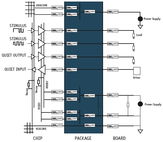
Figure 4. Cartoon view of the main circuit components simulated in a typical SSN analysis
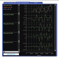
Figure 5. Waveforms from key points in an SSN circuit
Figure 4 shows the main circuit components simulated in a typical SSN analysis. It involves stitching together chip, package, board and I/O cell SPICE models and estimated parasitics, and then applying stimuli to buffer inputs, often sensitizing many pins of the I/O cell.
Figure 5 shows waveforms from key points in an SSN circuit. The top plot shows three waveforms from points along a signal line. Green is from the output pin of the buffer, red is near-end, and blue is far-end. The plots below show waveforms from I/O/core power/ground pins of the output buffer.
Having adopted this manual strategy, controlling SSN then entails either reducing the driver slew rate (which cuts di/dt) or the effective inductance (L). The following techniques and trade-offs are available.
Reducing di/dt
- Move simultaneously switching output pins away from each other, or swap them with quieter pins.
- Trade-off (TO): impacts pin placement, and adds SSN as a criterion for pin optimization.
- Reduce the driver strength.
- TO: impacts timing performance.
- Reduce the load driven by the pins, so driver strength reduction is possible without a loss in timing performance.
- TO: may not be feasible. Designers typically have little control over other components on the board.
- Set outputs to switch in a staggered fashion.
- TO: may not be feasible under the specification for the given interface standard.
Reducing L
- Increase the number of power/ground I/O pins on the chip.
- TO: may be impossible if all the pins are utilized already.
- Insert on-chip/off-chip decoupling capacitance.
- TO: all available space for decaps may already be in use.
- Choose a different package.
- TO: may be too costly or too late to change.
This methodology presents serious challenges and obstacles. Because the designer spends more time setting up the simulation than inspecting the results, there is little scope for ‘what-if’ analyses. Onchip parasitics are estimated manually and this is often insufficiently accurate for the simulation region. SPICE simulations have inherent capacity limits: designers cannot simultaneously simulate all pins of an I/O interface, but must simulate each piece individually.
Drilling down further into these limitations, we can observe that it may take one or two weeks’ worth of design cycle time to ensure that a manually-prepared netlist is correct. The team must undertake visual inspection of the netlist. Some 6-10 lengthy iterations may then be required to double check the content. After this, waveforms must be thoroughly inspected to finally confirm the validity of the pin sensitizations and signal shapes. And then, if another I/O region needs analysis, much of the manual setup and validation work must be repeated.
Automating SSN analysis
SSN analysis is not that different a design process from others that have already been automated. Moreover, tools that have a mature approach to full-chip dynamic voltage drop analysis (with support for package models), to parasitic extraction, and to basic design databases provide a strong foundation for dealing with this particular challenge.
Using the design database, a tool could automatically determine the I/O instances for a given simulation region in the layout and then how to appropriately sensitize or stimulate the pins. The region netlist, sensitization and stimulus information could then be applied to I/O cell SPICE models.
An accurate parasitic extractor could generate region parasitics for core and I/O power/ground rails. This data could be applied to the rest of the region.
A design database would provide information about the neighbors of I/O cells, so that topology-based activity patterns could be automatically generated.
The tool could automatically insert necessary reporting commands for the post-processing simulation output (e.g., generate eye diagrams, probe certain nodes), and invoke a simulator using the generated netlist.
Furthermore, coupling the design database and the simulation netlist with appropriate information would let the tool crossprobe waveforms from the layout of the simulation region. The user would be looking at the chip, thinking visually, clicking on the instances, and inspecting waveforms at the desired high level.
Because the solution has many components, the tool would need user-friendly debugging capabilities to inspect the automatically generated netlist for potential bugs. It would also have to validate the user-provided input (many models from many sources) and take errors out at an early stage.
The benefits that such automation could provide for SSN analysis can be summarized as follows:
Time savings
The simulation netlist for an I/O region could be generated in hours rather than weeks. Because automation minimizes human error, the number of iterations they cause could be reduced by about 90%. Each iteration avoided would save around a day’s effort. Because human error was minimized, time spent to debugging erroneous SPICE results would also fall by about 90%. Integrated and accurate parasitic extraction would eliminate the effort expended in developing a good lumped model for estimated parasitics. Another day, possibly two, saved.
‘What-if’ analyses
The time savings outlined above could free up resources to simulate additional regions, or more activity patterns in the same region, on a ‘what if ’ basis.
Improved accuracy
Integrated accurate parasitic extraction would eliminate the need for estimated on-chip parasitics.
High-level visibility
Integrated results post-processing, eye diagram generation and waveform cross-probing would let engineers spend more time on high-level analysis and decision making.
Improved capacity
If a high capacity simulator were used, designers could become independent of SPICE’s limitations.
In this context, Sequence Design has tailored its CoolTime dynamic voltage drop analysis tool to provides such an approach to SSN analysis with automated simulation netlist generation, integrated on-chip parasitic extraction, and waveform cross-probing.
Sequence Design, Inc.
469 El Camino Real
Suite 227
Santa Clara
CA 95050
USA
T: +1 408 961 2300
W: www.sequencedesign.com
