Asynchronous clocks prove tough for verification
For simulation to correctly predict silicon behavior, the logic implementing a design should adhere to the setup and hold constraints specified for clocked elements. However, with multiple asynchronous clocks on a single chip driving logic, designers cannot help but violate setup and hold constraints. This causes metastability, which in its turn leads to non-deterministic delays through synchronizers. For these types of designs it is critical that a designer has the tools to accurately simulate these non-deterministic effects while performing their functional verification.
Therefore, for designs that have asynchronous clocks, the traditional verification flow should be augmented with a comprehensive clock-domain crossing (CDC) verification solution that addresses the following:
- The complete identification of all clocks, CDC signals, verifying whether correct synchronizers are in place.
- The designer’s ability to verify whether the design correctly implements the CDC protocols that ensure uncorrupted data transfer between clock domains.
- The means to augment the simulation with behavioral metastability models (BMMs) to account for the non-determinism introduced by metastability and thereby accurately model silicon behavior.
The need tominimize power usage andmaximize performance is one of themain forces driving the use of multiple clock domains in SoCs. Not only do the functional blocks in today’s wireless, portable and multi-functional electronic devices operate on different frequencies, but inmany cases they will also be dynamically switched on and off by software to reduce overall power consumption.Many of these chips have 5, 10, sometimes even 20 ormore, independent asynchronous clock domains.
Digital simulation is one of the main methods designers use to acquire the confidence that chips have been designed correctly. It relies on abstract behavioral models of sequential and combinational circuits to describe the functionality of the design. When combined with static timing analysis that ensures a required functionality is achieved within the available timing budget, simulation has proven to be an excellent predictor of silicon behavior – that is, as long as the design is driven by a single master clock.
When this is not the case, simulation falls short because one of its fundamental rules is violated. The rule states that a design should adhere to the setup and hold constraints specified for clocked elements. For synchronous designs, this is exactly what static timing analysis verifies – that, given a particular clock frequency, the setup and hold constraints are met. Only when a design passes timing can one rely on the simulation results. However, when multiple asynchronous clocks drive chip logic, designers cannot help but violate this basic design rule.
Any time data is transferred between asynchronous clock domains, the clock-domain crossing (CDC) signals carrying this data will at some point violate the setup and hold constraints specified for the receiving registers.When this happens, the flip-flops in these registers may become metastable—they will not settle to either a logical ‘1’ or ‘0’ within the specified delay for normal operation.
To prevent metastable signals from propagating through the design, designers have devised specific circuits, called synchronizers, to connect asynchronous clock domains. However, synchronizers do not eliminate the occurrence of metastability; rather, they reduce to almost zero the probability that metastable values will contaminate the rest of the design.

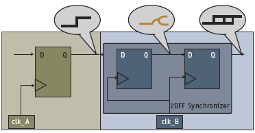
Figure 1. When asynchronous clocks A and B are closely aligned, the first flip-flop in the 2DFF synchronizer can go metastable. The synchronizer confines the metastable signal but has a non-deterministic delay.

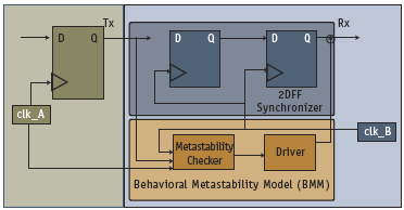
Figure 2. By adding a BMM to a synchronizer, the simulation will correctly reflect the non-deterministic delays of synchronizers.
With synchronizers connecting clock domains, the occurrence of metastability is observed as a non-deterministic delay. For example, in silicon, the delay through a common dual flipflop (2DFF) synchronizer can be one, two, or three cycles (Figure 1). Simulation, a deterministic process, always produces a two-cycle delay.
Simulating synchronizers correctly
So, we have seen that simulation falls short because it does not model the behavior of synchronizers correctly. To correctly simulate the behavior of a synchronizer (with respect to silicon), simulation must show the non-deterministic behavior of the synchronizer. When the setup constraint for a synchronizer is violated, simulation should randomly add a cycle delay, and when the hold constraint is violated, it should randomly subtract a cycle delay. Only in this way will it correctly reflect silicon behavior.
To accomplish this, designers could create separate primitive behavioral models for each type of synchronizer. This, however, is not a practical solution because designers use many different kinds of synchronizers. A more practical and fundamental solution is to add behavioral metastability models (BMM) to the synchronizers (Figure 2).
A BMM consists of two parts: a checker that recognizes when setup or hold constraints are violated and a driver that randomly overrides the output of the original synchronizer (modifying the delay through the synchronizer). A BMM can be automatically implemented in the standard sequential and combinational primitives that the simulator already supports. Only when BMMs are added to a synchronizer, does one have an accurate functional model of the silicon.
The complete solution
Manually adding BMMs to a design is labor-intensive and errorprone. Moreover, changing a design solely for the sake of making it simulate correctly is generally not allowed. Thus, we require an automated solution that correctly deals with asynchronous clock domains.
Since all CDC signals need a synchronizer, the first part of a complete solution consists of extensive structural or static analysis of the RTL code to identify all CDC signals and ensure that the proper synchronizers are in place. Any complete solution should also automatically identify the various clock domains, map the clock distribution strategy, and recognize the wide range of synchronizer structures designers use to connect clock domains. Once it is determined that the right synchronizers are in place, designers must verify that data is transferred correctly across them. For most types of synchronizers, the design has to adhere to a particular protocol, generally referred to as a CDC protocol. For example, if a value change has to be transferred from a faster to a slower domain, the signal must be kept stable long enough (in terms of the slower clock) for it to propagate through the synchronizer even when metastability conditions are present. The best approach is to automatically generate these protocols as assertions when running static analysis. Since CDC assertions typically specify properties for the logic in the originating clock domain, traditional simulation and formal analysis are very effective at verifying that the design obeys CDC protocols.
The last step is to verify that the non-deterministic delays of synchronizers are handled correctly by the design. To obtain a simulation that truly reflects silicon behavior, the designer needs to instrument the design with the BMMs for selected synchronizers.Mentor’s 0-In CDC verification solution automates this process.
First, the tool analyzes the RTL code and determines the set of synchronizers for which the non-deterministic delays could cause a problem. This is referred to as ‘structural reconvergence’ analysis.

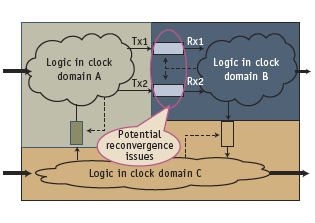
Figure 3. The 0-In CDC verification solution automatically determines where non-determinism in synchronizers could cause a problem in the design.

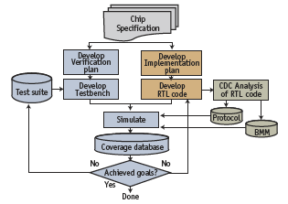
Figure 4. Verification flow for designs with asynchronous clocks: while developing the RTL code, engineers run the CDC analysis and generate the BMMs that are subsequently included in simulation.
In Figure 3, for example, two synchronizers between domain A and B are clocked by the same clock (B), and both signals Tx1 and Tx2 are clocked by a different clock (A). Since regular simulation is deterministic, both Tx1 and Tx2 will simultaneously either violate the setup constraint or the hold constraint. In other words, during regular simulation both synchronizers will always simulate with the same delay. In silicon, however, the delays through the two synchronizers are independent and, therefore, can be different. The only way to verify that the logic in domain B deals with these non-deterministic delays correctly is to augment the synchronizers between domain A and B with BMMs.
The 0-In CDC automatically recognizes these scenarios. For the scenario shown in Figure 3, it will generate the BMMs for the synchronizers between the A and B clock domains, and will also determine that regular simulation will suffice for the lone connections between the A and C clock domains and the B and C clock domains.
The general rule to determine whether BMMs are needed is:
When two or more pieces of data have a well-defined timing relationship in clock domain A, and are moved through separate synchronizers to clock domain B, that timing relationship can no longer be relied upon in domain B.
Using this rule, 0-In CDC locates all parts of the design where reconvergence issues may be present.
The second phase of reconvergence verification is then to add the BMMs to the simulation. This is automated in 0-In CDC as well.
Furthermore, the tool automatically collects coverage data on the BMMs. This is very helpful because it outlines exactly where and when metastability conditions occurred during a simulation and whether a BMM modified the original simulated delay of the synchronizer.
Verification flow for designs using asynchronous clocks
With many of today’s wireless,multimedia, computing, and communications designs using asynchronous clocks to optimize power and performance, leading companies have started to integrate CDC verification as an integral component of their verification flows. The complete solution described above fits easily into any existing verification flow. The same testbenches can be reused, only now they use an accurate model of the design-under-test. The coverage information collected on the CDC protocol assertions and BMMs further guides the verification flow as it pinpoints where the effects of metastability have been simulated and directs test development to ensure full functional coverage of the design. Applying a comprehensive and effective verificationmethodology (Figure 4) for designs that have asynchronous clocks is critical tominimize the verification overhead whilemaximizing the identification of CDC problems. Key components should include:
- Block Design. During block design, CDC static analysis should be run whenever major code changes are made. This identifies structural problems and potential block-level reconvergence issues prior to the availability of a testbench.
- Block Verification. The generated CDC protocol assertions and BMMs should be included during block-level verification to ensure that CDC protocols are followed and to ensure that the silicon behavior of the block is modeled correctly.
- Chip Integration. Static analysis should be re-run during chip integration to check CDC signals created when multiple blocks are integrated. This may lead to new CDC protocol assertions and chip-level reconvergence issues.
- Chip Verification. Engineers usually build their regression suites during chip-level verification. Both the CDC protocol assertions and BMMs should be included in those suites. Coverage should be checked and, if necessary, additional tests created to fill any coverage holes.
Conclusion
With respins costing millions of dollars in engineering cost alone, not to mention the cost of delayed product introduction, you simply can not afford to miss bugs. Therefore, correctly and completely modeling metastability is a must for any design that uses asynchronous clocks.When equipped with tools that can automatically complement existing simulations with behavioral metastability models, engineers are able to accurately simulate silicon behavior and achieve the highest level of confidence that the chip will work before it is sent to the foundry.
Mentor Graphics
Corporate Office
8005 SW Boeckman Rd
Wilsonville
OR 97070
USA
T: 1 800 547 3000
W: www.mentor.com


