Assessing the true cost of node transitions
 John Ferguson is the Director of Marketing for Calibre DRC Applications at Mentor, a Siemens Business, with extensive experience in physical design verification.
 Moore’s Law has held largely true for more than 50 years (Figure 1). During that time, a new process node (commonly defined by the smallest possible transistor pitch for a manufacturing process) has been established roughly every 18 to 24 months. With a smaller transistor size, designers can incorporate more transistors per die area, increasing total compute power node over node. But the economics behind moving from node to node are becoming more complex.
![Figure 1: Moore’s law has held relatively steady for over 50 years [1].](https://www.techdesignforums.com/practice/files/2017/11/Fig1_Moores-Law.png)
Figure 1: Moore’s law has held relatively steady for over 50 years (Click image to enlarge)
Implied by Moore’s Law are the economic benefits of node migration, as defined by changes to manufacturing costs. Decreasing the size of the transistor means the total number of transistors per area can be increased. This relationship reduces the total cost per transistor, and has therefore made node migration particularly attractive.
We have also periodically seen increases in the total wafer diameter used by foundries (Figure 2). This has also had a historically positive impact, since fitting more chips on each wafer reduces the aggregate manufacturing costs.
![Figure 2: Increasing wafer size reduces the manufacturing cost per chip [2].](https://www.techdesignforums.com/practice/files/2017/11/Fig2_Wafer-sizes.png)
Figure 2: Increasing wafer size reduces the manufacturing cost per chip (Click image to enlarge).
Of course, other mechanisms counteract some of these economic gains. As we squeeze more and more transistors into the same area, we have less room to connect between them. This has required an increase in the total number of metallization layers (Figure 3). That in turn has had an impact on both the manufacturing costs (more masks are required to manufacture the full chip), and the chip’s electrical design (more power is required to push the signals through so many layers of metals and vias).
![Figure 3: The increase in metal layers increases manufacturing cost and complexity, and impacts chip electrical behavior [3].](https://www.techdesignforums.com/practice/files/2017/11/Fig3_Increase-in-layers.png)
Figure 3: The increase in metal layers increases manufacturing cost and complexity, and impacts chip electrical behavior (Click image to enlarge).
So, if you examine a 20nm process, you will be hard-pressed to find any device geometry pitch that is actually 20nm between components. From the 28nm to 20nm node, the change in minimum transistor pitch has not nearly been as large as the expected 8nm. While the number of transistors that can be placed in a given area continues to improve for each full node transition, the cost of achieving that area reduction is now rising at a much higher rate than before.
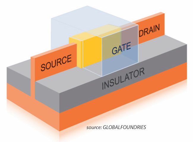
Figure 4: The introduction of finFET transistors changed the definition of node scaling (GLOBALFOUNDRIES)
At 20nm and below, our ability to accurately print the finFET device fins and other fine-grained structures faces very challenging lithographic limitations. This manufacturing issue was first addressed with double patterning. We now have various multi-patterning techniques to mitigate the lithographic impacts of printing in dense regions by splitting layout geometries across two or more masks. Of course, each mask comes at a considerable price to both the design and manufacturing processes (Figure 5) in terms of additional time, staff, and resources.
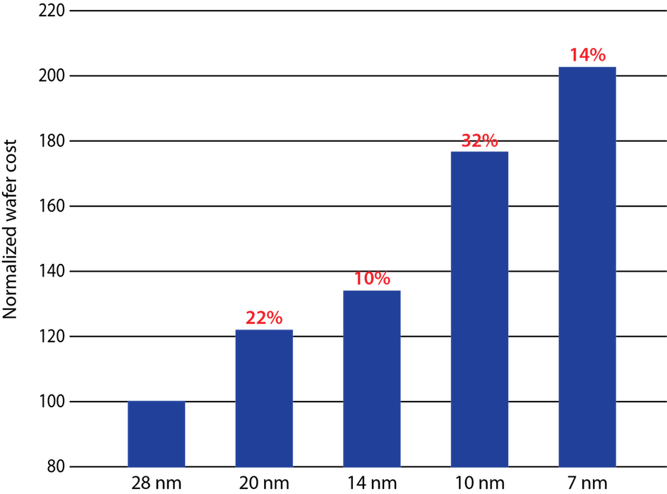
Figure 5: Normalized wafer cost trend – node to node evolution.
Because manufacturing costs typically decline after a process’ initial introduction, taking a long-term view can help a company undertake a manufacturing cost/benefit analysis over the expected lifetime of a node. However, the company can fail to consider other financial implications associated with any decision to move to a new node.
Design flow costs
Manufacturing changes are not the only source of economic disruption when migrating to newer nodes. Less commonly acknowledged factors include increased costs to design.
With each new node, new manufacturing processes manifest themselves as new design constraints (Figure 6). For example, more design rules are needed to accurately account for the parasitic impacts of metallization when characterizing a chip’s performance; or to analyze device context to capture stress impacts upon the behavior of each transistor; or to split a dense layer to two or more masks properly.
More design for manufacturing (DFM) analysis is required to predict the impact of manufacturing limitations in processes such as lithography and chemical-mechanical polishing (CMP).
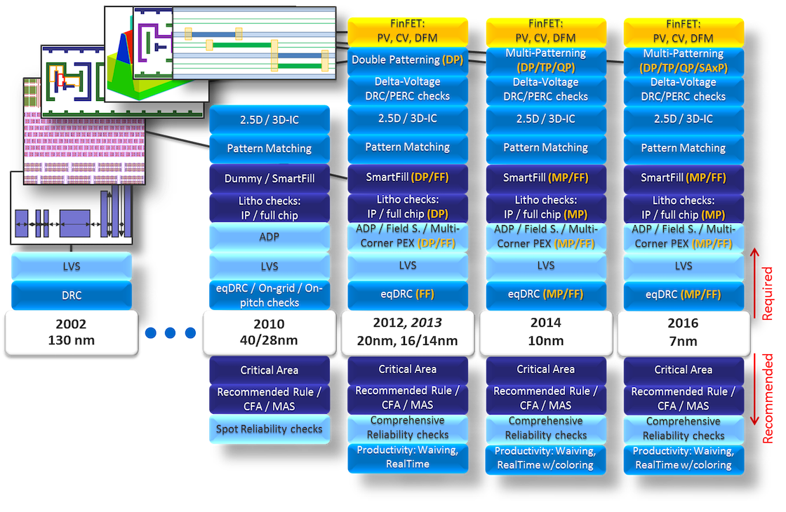
Figure 6: Design requirements have increased significantly node over node for physical and circuit verification, as well as DFM optimization (Click image to enlarge)
These tighter constraints alter many parts of the design flow. Existing EDA tools may change. New tools and/or flows may also be required. That will often require extra designer training.
The new constraints will then typically increase the total time required to take a design from concept to tape-out, and require significantly greater computational resources. These issues will increase the costs associated with both increased hardware and the corresponding increase in your compute farm’s power and cooling infrastructure.
We can get a sense of the significance of these impacts by looking at the evolution of design rule checking (DRC) across the process nodes (Figure 7). With each new target, the total number of design rules required for sign-off increases dramatically. Equally noticeable is the increase in the number of DRC operations required to implement these rules, reflecting their increased complexity.
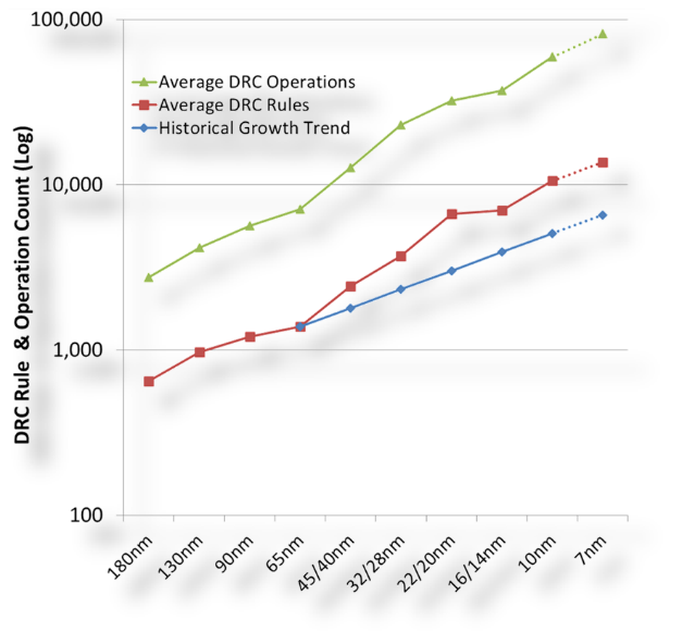
Figure 7: Average growth in design rules and DRC operations over node progressions.
When these DRC increases are taken into accounted for alongside those related to increases in the number of layers, the physical sizes of the chips, and the total geometry data, we can better appreciate their combined effect on the computing requirements for each node (Figure 8).
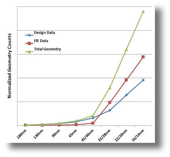
Figure 8: Multiple growth factors, like the exponential growth in total data, impact the time and costs of node progression.
Meanwhile, as the computational burden increases, so does that for human resources. With ever-increasing complex designs, the number of designers needed for both analog/custom and digital implementation grows when moving to advanced nodes. In analog/custom designs, staffing need is being driven by the rapidly growing number of AMS blocks in an SoC, the increasing number of complex circuits in nm-node analog, more power-saving modes, and so on. Over the last 5 years, one has then commonly heard of 50% node-over-node IP designer staffing increases.
Tool and hardware performance costs
The costs associated with physical verification tools are often measured solely on the basis of completing full-chip verification in what the user considers a reasonable runtime. While faster processing of design rules on faster hardware is essential, even that may not be enough to achieve an acceptable runtime unless combined with efficient hardware scaling and distributed processing across multiple CPUs. However runtime is determined, continuous performance enhancement and efficient hardware scaling (i.e., more resources) are critical to meeting runtime goals at all nodes, but especially at advanced ones.
While verification tool platform developers continuously improve the speed and efficiency of their engines, enhance flows, and partner with the foundries to optimize manufacturing rule decks, an exponential node-over-node increase in the computational requirement means scaling up farms is the only remaining means of maintaining constant turnaround times (Figure 9). Depending on design size and runtime targets, tools that can scale up to thousands of cores will operate with greater efficiency.
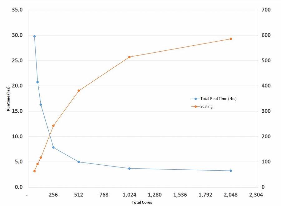
Figure 9: Verification tools must operate efficiently by scaling up to thousands of cores, depending on design size and runtime targets.
EDA companies work closely with foundries to understand the technological requirements of each node and ensure the core verification functions in the tools work with the decks as the industry moves forward. This helps ensure customers can confidently port their existing installations to new versions that have the necessary functionality and performance for the new node. Design companies that use the same verification tools as their foundry’s ‘plan of record’ toolset can even move ahead with new process node designs without waiting for tool qualification.
Another consideration is how you access advanced verification tool functionality. For example, multi-already now frequently used at advanced nodes to identify complex layout configurations prone to lithographic hotspots.
However, fabless designers can be reluctant to adopt such software if it is not mandated by the foundry, while foundries can be reluctant to implement rules that may require their customers to obtain new software. EDA companies can make advanced functionality available on an as-needed basis, so that customers acquire only what they need. Multi-patterning, pattern matching, advanced fill technology, advanced reliability checking—all of these capabilities and more can be readily adopted and implemented on an ‘as needed’ basis.
Of course, software costs do not show the total design cost impact of a node migration in isolation. The total hardware costs must also be considered. A true understanding of the total cost of physical verification from a hardware point of view must address the number of processors needed over the course of a design flow. Once that number is understood for each tool, then the total cost for each tool can be calculated.
It is critical to consider not just the price per processor, but also additional one-off and recurring hardware costs. Consider these examples:
- The total cost to purchase appropriate hardware can vary dramatically depending on specific requirements, such as:
- Number of processor nodes
- CPUs or cores per node and corresponding availability of virtual cores
- RAM required per node
- Disk storage required
- Network configuration required
- Rack housing architecture to hold the nodes
- The recurring cost of supporting the hardware can vary according to factors such as:
- Hardware vendor support cost;
- Internal IT support cost.
- What are the licensing and support costs associated with grid queuing and allocation software?
- What are the recurring electrical costs of powering the processor farm configuration?
- What are the fixed and recurring costs associated with cooling the processor farm.
- What are the real-estate costs of housing a processor farm.
The fixed cost of the hardware can vary greatly, depending upon the requirements of the specific verification software. In the past few years, the cost of processors has fallen significantly, and this trend appears to be continuing. It is now economically feasible to purchase a single machine with more than 64 physical cores. Such an approach can help to reduce total housing and related costs.
In addition, for advanced node, large, full-chip designs, physical verification runs may require significant RAM. The total amount of RAM that can be housed on a node is associated with the number of available dual in-line memory modules (DIMMs) in the system. Having access to such large devices also ensures a large number of DIMMs to better ensure sufficient memory is available for the job (Figure 10).
Also, the most effective use of a compute farm does not have to (and should not) be limited to one function, like physical verification. To make the best use of multiple processors, consider all the design and corporate software functions that the farm can support. A variety of hardware and software innovations helps ensure fast verification runtimes for all designs at all nodes. Users should work with qualified hardware vendors who have the expertise to ensure that they make the best of all their resources.
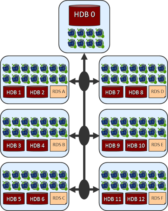
Figure 10: Distributed processing configurations enable the most efficient scaling of both data and rule operations.
One approach interesting many users is the use of cloud computing to replace in-house hardware. Particularly for off-peak cloud hours, the costs can often be essentially equivalent to the costs of self-owned server farms, but without the hassles associated with their infrastructure (real estate, power, cooling, etc). On the other hand, users must be able to count on access to sufficient cloud resources at the time they need them, not just during low-demand or off-peak times. In addition, cloud computing is still considered risky by many design houses due to uncertainty of the security levels protecting their data.
Making that node decision
When migrating to a smaller node, there is always an increase in total cost, due to the need to run more complex tasks, often requiring more licenses, newer licenses, and more hardware. When migrating to the most advanced process nodes, the cost often increases dramatically due to the increased cost per mask, the increased total number of masks required, a significant bump in required hardware and tool licenses, and the fact that the reduction in die areas has been lost.
In these cases, migration is primarily predicated on the design’s need to meet faster performance and/or lower power metrics. Interestingly enough, there are still plenty of markets where these characteristics are attractive are still plentiful, with many design houses targeting process nodes at 16nm and below.
How do you make the best decisions on the software and hardware you use? You need to balance all of these factors, and that may lead some companies to more carefully consider the true long-term cost/benefit analysis of a node transition.
In the end, the solution that requires the least amount of total change—in the form of license configurations, required hardware resources, necessary tool qualifications, and adequate support infrastructure—will always be the most “inexpensive” option. At the same time, ensuring that your verification platform provides the performance and the foundry-qualified technology you need to advance from node to node will deliver the confidence you and your customers demand that the tools you use for today’s designs will be equally accurate, efficient, and comprehensive when addressing tomorrow’s requirements.
