ARM, TSMC design explores 16nm finFET issues
ARM and TSMC used an extensive pre-planning process, including a static analysis of each module’s overall logic structure, to put together a 2.3GHz processor design based around ARM’s main 64bit Big.Little pairing for the foundry’s 16nm finFET process.
Chek-San Leong, IP ecosystem manager at TSMC, explained in a session at ARM TechCon this was a second-generation test chip for the finFET process with targets intended to mimic those of expected production implementations. “All the targets were very close to those expected for real smartphone implementations,” he said. “It has on-chip power switches, support for under-drive and overdrive and full manufacturing test support.”
Leong claimed: “The finFET process gives you a very good performance gain compared to planar. However, it imposes a number of challenges. One of the key challenges will be dynamic power, which does not scale as well as the leakage power. This created a lot of implementation challenges for the team.
“High pin capacitance also imposes a number of challenges as does device tuning because basically everything in the finFET is quantized. This imposes big challenges for the analog design and also for the SRAM design because read margin has to be carefully controlled. With 16FF you have to spend a lot of time on read and write design [for SRAM arrays],” Leong said. “And we need to adopt a new sign-off methodology: stage-based OCV.”
Standard-cell implications
For the logic design, double patterning issues caused the team to look hard at standard-cell architecture and the way logic synthesis uses the available cells. “A smaller call doesn’t mean smaller area,” Leong said, showing one typical high-density cell. “When it abuts to another cell it creates DRC errors and routing problems because it has insufficient pin access. So, you need to enlarge the cells for better pin access and allow them to abut more easily.
“For 16nm finFET we have to look at the design carefully,” Leong said, using both static analysis and dynamic techniques. “We did static structure analysis to look at each module of the design, to understand whether the module is logic or memory dependent. For runtime behavior we run code such as Dhrystone to understand the behavior of the module, as well as test vectors to understand where the dynamic [power] hotspots of the design are.
“At the same time we did a lot of exploration to understand the PPA characteristics of each of the libraries. We set different targets for each of the blocks. If a block is not timing critical then the goal is [primarily] leakage optimization. We used HVt [high-threshold voltage] libraries for those. For timing-critical path we we used LVt [low-threshold] and also used smaller cells to try to meet timing. If a block had lots of registers, its timing is [unlikely to] that critical. So we used multibit flip-flops for those,” Leong explained.
Synthesis tuning
The standard optimizations used by synthesis tools tended to favor the use of dense, small cells because they typically offer less internal delay. As these cell tend to have high pin counts, they make “routing very challenging, which creates routing resource problems. We also faced large delays caused by the need to include buffers along the logic paths. The engineering team analyzed these paths and, if there was an opportunity to replace a high pin-count cell, it was broken into several [simpler cells]. The individual cell delay is larger but the overall total delay is shorter. So, to reduce the RC impact [from the interconnect] and improve timing, we used multiple small cells rather than big cells.”
The team chose to use nine-track cell libraries – one from ARM and one from TSMC allocated to different parts of the design – rather than the fractional architecture supported by ARM.
Leong said the team favored the use of fast combinational logic over fast flip-flops where there was a choice between those options. To deal with dynamic-power hotspots, the team performed logic optimizations based on switching activity. “Also, allowing lower-Vt cells for for synthesizing dynamic hotspots leads to great reductions in dynamic power for a small increase in leakage power,” he said, using cells such as ULVt D1 rather than LVt D4.
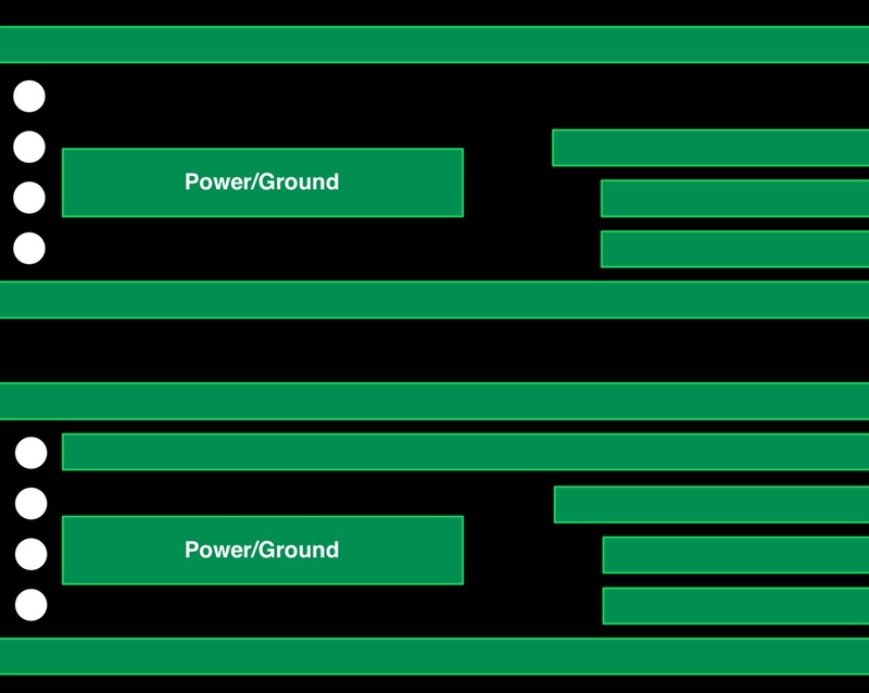
Image Subtle misalignments in power routing can block more signal tracks (top) than expected (below).
The increasing power density of 16FF designs relative to the 40nm and 28nm generations cause problems for die utilization in two ways. One is simply the increased competition for metal from the power rails and signal tracks because the die should be half the size of its 40nm equivalent but expected to double performance from 1GHz on 40nm to 2GHz or more on 16nm. “The effective power-metal area that can be packed into the design is much less than for 28nm or 40nm,” Leong said. “But you also need to look at the power structure carefully. You need to find the right metal length and spacing in order to not waste routing tracks.”
“Because this project was built last year, the PDK was at version 0.5. Things like EDA tools could not deal with
such complex power structures,” said Leong. So, to avoid blocking too many signal traces with power rails that do not align well with the fin layout underneath, the team had to carefully analyze the layout and modify it.
“ARM is now launching the Power Grid Architect. So the issue can be resolved by flows and tools,” Leong claimed.
“A lot of time the engineers had to do more manual work to free up routing resource for design,” Leong said, adding that improving density to hit physical closure targets was problematic in general. “We took two different tactics to resolve highly congested area. We went back to synthesis stage to see if there was any way to optimize the logic to fix congestion. And we also used instance-padding. If you are too aggressive you hurt your routing resource.
Clock-tree design
“For the clock tree, there a couple of rules we strongly recommend. You need to use [upper-layer] metal as much as possible to minimize resistance and reduce variation. We used non double-patterned layers for the clock tree,” Leong said. On this design, the clock tree was routed using M4-M7. Although TSMC provides the option of a denser M4 using double patterning, M4 was single-patterned on this design. The use of single-patterned layers minimized variation significantly, Leong claimed. “We also used manual placement of ICGs and anchor buffers. If the tools do it for you, it can be difficult to close timing.”
To limit the amount of time needed to perform timing signoff, the design team pre-screened corners to work out which would have the biggest impact. “You need to find out what are the dominant corners for your design when you do design optimization. There is no way you can cover design by using a high number of corners because runtime will be too long. Do prescreening to understand how the design behaves: it could be wire or device dominant delay,” Leong said. For the project, the team ran 15 corners with two for primary signoff aimed at either end of the temperature scale.
To take account of effects such as back-Miller capacitance on the signal waveform, the procedure employed waveform propagation. “Before, at 28nm, this was the recommended flow. But at 20nm and below, this is a must,” Leong said. “We worked with the physical IP team very closely. Every day the two teams talked to each other to understand all the issues.”
Post-silicon, the 16FF design met its predicted timing envelope with some margin at all its voltage settings. TSMC has gone on and performed the same exercise for the improved 16FF+ process. “On early simulation of 16FF+ for same power envelope, the frequency on the big core increases 11 per cent. The little core can go up to another 35 per cent down in voltage. We haven’t taped out that test chip yet but we believe it will be very close to the [predicted] line. We believe TSMC and ARM are the industrial leaders,” Leong claimed.
