Accelerating the move from prototype to production with a robust design flow
When migrating from FPGA prototype to ASIC, engineers need to interface with multiple silicon and software vendors. Designing with FPGAs often requires the use of several software platforms, including front-end synthesis tools, FPGA software development tools, and verification and timing analysis tools. Migrating to an ASIC platform involves using a parallel design flow with different sets of front-end tools for synthesis and back-end tools for place and route, timing closure, equivalency checking, layout, and the design rule check.
Substantial tool licensing costs and staffing resources are required to manage and execute a design under these conditions. The complexity of the process can also contribute to delays in time-to-market and to the inflation of development costs. The total development budget for a single, complex, high-density standard cell ASIC can fall between $20m and $30m at the 90nm process node.
Furthermore, inefficiencies such as a lack of tight tool integration prevent engineers from optimizing the design for all environments. Portions of their code often require redesign due to incompatibilities in the silicon architectures, such as embedded memory structural differences. This problem is compounded by the different register-transfer level (RTL) coding styles required when targeting FPGA against ASIC architectures. In addition, pinout differences between FPGAs and ASICs often require a printed circuit board (PCB) respin when migrating from one platform to the other.
Such obstacles to design portability reduce productivity levels and lead to low first-time-right design success as well as product delays. Engineers must often perform ASIC respins, increasing engineering and mask-set costs, and potentially causing significant lost market opportunity.
Minimizing risk with an FPGA-to-structured-ASIC flow
Using FPGAs for prototyping and then migrating to structured ASICs for production can help reduce development costs and mitigate design risks. Designers can use FPGAs to minimize the upfront investment because these devices have no non-recurring engineering costs (NREs). They also use FPGAs to perform in-system verification to fix design bugs, remove technical risk, and demonstrate their technology to customers prior to device production.
Manufactured on leading-edge processes that meet a majority of new ASIC or ASSP design-start requirements, FPGAs can offer core performance in the hundreds of megahertz range, I/O performance in the gigahertz range, densities of millions of gates, and costs ranging from under $10 to nearly $1,000 per unit.
These devices allow designers to get a head start on system development and qualification with customers in the field, thereby removing market risk while ensuring customer acceptance of the product. This added flexibility lets companies take the time to test the market and customize their products. Thus, it even becomes possible to simultaneously release multiple variations of an original design optimized for different markets.
Under such a scenario and with the flow we describe here, we intend to show that, as product demand increases, designers can move seamlessly from FPGA prototype to a footprint-compatible Altera HardCopy series structured ASIC device without respinning the board.
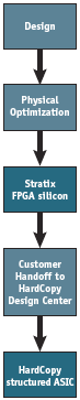
Figure 1. HardCopy ASIC development flow
This strategy provides both a fast track to production (the turnaround time is measurable in weeks) and upfront NREs that are a fraction of those associated with standard cell ASICs. This development flow means that engineers can undertake design work just once for both the FPGA and the structured ASIC, bypassing the pain and expense of traditional ASIC development while still meeting cost, performance and power targets.
The seamless prototype-to-production flow available with Altera’s HardCopy devices simplifies design. Engineers simply create and optimize their design for the FPGA and verify the design in-system. Then, they create an archive file to hand off to the Altera HardCopy Design Center. ASIC prototypes are delivered in record time (Figure 1).
The flow includes several significant features aimed at reducing the technical risks of Stratix II FPGA to HardCopy II structured ASIC migration:
- Several ‘hard’ intellectual property blocks such as phase-locked loops (PLLs), clock trees, embedded memory blocks, and I/O blocks are common to both the Stratix and HardCopy families.
- Both device families are manufactured using the identical TSMC 90nm G process technology and offered in packages with the same footprint.
- A single integrated software tool environment is used to design for both devices.
- The Quartus II v6.0 design software suite features several new automated conversions that minimize errors when migrating designs. Additionally, Quartus II software remaps the FPGA netlist when creating a HardCopy netlist without resynthesizing the design, ensuring functional equivalency.
Application of methodology using Altera and Mentor Graphics tools
To resolve the productivity and design optimization challenges faced by hardware engineers, Altera and Mentor Graphics have developed a robust design methodology, shown in Figure 2.
Hardware designers can create and manage their designs and constraints in Mentor’s HDL Designer Series and synthesize design using Mentor’s Precision RTL Synthesis software. Precision synthesizes RTL code based on user constraints and generates a synthesized netlist that is optimized to the targeted Altera FPGA architecture. This software can recognize high-level structures, including memory and digital signal processing (DSP) functions, and map them directly to the dedicated logic structures in Altera FPGAs. Constraints from the Precision synthesis are then forwarded directly to Altera’s Quartus II software.
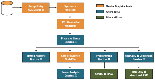
Figure 2. Altera/Mentor Graphics integrated tool flow
Quartus II performs place and route on the design, and generates a gate-level netlist for simulation with Mentor’s Modelsim simulator, as well as a programming file that can be used to configure the FPGA. The entire design flow between the Mentor and Altera design environments can be automated using tool command language (Tcl) scripts. This allows designers to perform a wide range of tasks, such as compiling a design or writing procedures to automate common tasks.
Migrating the design to a HardCopy structured ASIC device is simple once the design has been completed in a Stratix FPGA. HardCopy structured ASICs maintain the same pinouts as the corresponding FPGA so that no PCB respin is required. The same PCB design and verification project files and models can be used for both Stratix FPGA and HardCopy structured ASIC implementations. Using a single design for both the FPGA and ASIC improves productivity and time-to-market.
Team-based design
Medium- to large-scale designs will often require more than one engineer to design and implement the design blocks. Various teams working in different locations are now the norm, especially for high-end ASIC design work. The Mentor Graphics/Altera methodology supports this team-based approach, allowing each logic block to be individually developed, optimized and locked down so that the design is created one block at a time.
Constraints can be used either with custom blocks of logic or with pre-verified IP. The FPGA design flow guarantees repeatable placement when implementing a module of logic in a current project or exporting the module to another project. This methodology ensures that the performance of each block is preserved during system integration. In turn, this reduces the number of design iterations and mitigates risk. Additionally, design blocks can be reused in other designs, further leveraging resources and shortening design cycles.
Automated design flow
Where there are large device pin-out counts and small pin spacing, several factors can influence whether or not physical pin numbers are successfully assigned to the ports of each FPGA design. These factors include the routability of the FPGA, placement of the FPGA relative to its neighboring components on the PCB, system interface location constraints, and PCB routability. Tools such as Mentor’s I/O Designer software and Quartus II help designers to make tradeoffs between the FPGA and PCB designs by automating the flow between the FPGA and PCB tools. This reduces the risk of error and simplifies design.
System Debugging
Occasionally, hardware and firmware engineers must debug incorrect memory states or force incorrect memory conditions to [MISSING WORD] test error handling. Engineers need the ability to read, write, dump and initialize memory in their designs. Proprietary FPGA design software provides read and write access to in-system FPGA memories and constants through the Joint Test Action Group (JTAG) interface, making it easier to test changes to memory contents in the FPGA while the device is functioning in the end system. The ability to read data from memories and constants allows the hardware engineer to quickly identify and fix the source of problems, helping them deliver working product to the market as quickly as possible.
Conclusion
In today’s market, with increasing competitive pressures and shorter product life cycles, designers have less time to develop and differentiate higher performance, more complex designs. At the same time, the development cost of an ASIC is dramatically increasing, making it less feasible to use the technology for many cost-sensitive applications.
To overcome these hurdles, companies must consider a business model that enables a cost-effective design methodology flexible enough to allow quick changes within this unstable market environment.
As time-to-market and cost reduction pressures intensify, the combination of Altera FPGAs and HardCopy series structured ASICs, together with robust software tools from Altera and Mentor Graphics, give designers the ability to create a single design for both prototyping in an FPGA and production in a structured ASIC. This low-risk, low-cost design solution addresses a majority of volume applications while ensuring the fastest time to market.
Altera Corporation
101 Innovation Drive
San Jose
CA 95134
USA
T: +1 408 544-7000
www.altera.com
