20nm
The 20nm node can offer power, performance and area advantages, but making these gains takes a deep understanding of the interactions between process and design.
The introduction of copper interconnect coupled with low-k dielectrics in the early 2000s allowed the continued scaling of semiconductor processes. Copper’s higher conductivity compared to that of aluminum and the lower dielectric constant of the insulator contributed to a temporary halt in the increase of RC delay that threatened to derail performance improvements from the core transistor.
During the past ten years, interconnect dimensions have continued to scale leading to an increase in overall wire length – a three-fold increase since the 90nm node – coupled with increases in resistance and capacitance from increasingly closely spaced, thin wires. Foundries were able to reduce the contribution to RC delay from resistance by increasing the aspect ratio of the interconnect – with a resulting increase in coupling capacitance – as resistance has become an increasingly difficult problem to solve.
For the sub-32nm generations of processes, interconnect resistance is set to rise dramatically. As well as ‘classical’ reasons for higher resistance, such as the reduced cross-section of the wires, other effects are coming into play. As predicted by the International Technology Roadmap for Semiconductors in 2007, at and below 22nm, carrier scattering from the boundaries of individual copper crystal grains and the interfaces with barrier layers that separate the conductor from the dielectric is rapidly pushing up interconnect resistivity and, with it, the resistance of individual wires.
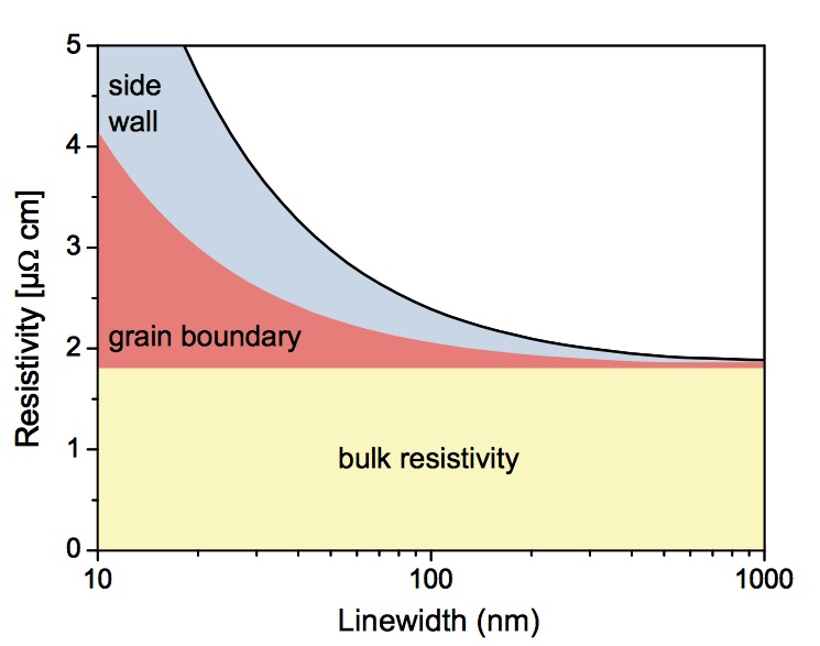
Figure 1 Sources of copper resistivity due to scaling (Source: ITRS)
According to EDA tools providers such as Cadence Design Systems and Synopsys, the difference in resistivity can be 100-fold between the top and bottom metal layers.
One method for reducing wire resistance is to provide wider interconnect traces on the lower metal layers for critical nets that cannot suffer the higher RC delay of the ‘normal’ wires. However, the introduction of double patterning introduces problems for this approach as the inclusion of the wider wires can introduce problems for mask coloring and, therefore, the clean separation of the design into two complementary masks, as indicated by Jim Warnock of IBM at ISPD 2013. In the example in Figure 2, because of the requirement for consistent pitch spacing of double-patterned metal lines, the use of a wider trace leads to the need for an adjacent line to the fast wire to be ‘stitched’ – that is, the line needs to cross from one mask to the other, which may lead to yield loss from misalignment as well as incurring more design overhead.

Figure 2 Double-patterning mask-color problem caused by the use of a wider wire (Source: IBM)
A further complication lies in the local-interconnect layer introduced in the 20/22nm generation of processes below metal one. The resistance of this local interconnect is highly dependent on interconnect topology – changes in the placement of vias within a given trace will alter the resistance of the resulting wire.
Foundries appear to have chosen the route of using upper-layer metal interconnect instead to provide fatter, faster routing for critical nets. Even the upper metal layers could be used, although this will lead to competition for resource with power and clock signals that are normally allocated these layers to reduce the risk of failure from electromigration and clock skew.
However, the tradeoff between using the scarce resource of upper-layer, low-resistance metal is less than straightforward. At IEDM 2013, Qualcomm’s Geoffrey Yeap showed that interconnect performance is more sensitive to via resistance than that of the wires. Pushing a signal up through a number of vias may simply exacerbate the problem caused by high resistance on thin lower-layer wires.
The use of non-uniform metal layers drives a demand for layer-aware interconnect routing and synthesis, using accurate models of resistance and RC delay to guide the tools to use lower-resistance routes for critical nets and to alter placement to take account of congestion in the layers that offer wider, less densely packed interconnect.
A key to making effective use of lower-resistance routing is to ensure that it is only used for nets that need it, to avoid causing excessive congestion in the middle and upper layers. Cavium and Synopsys described their approach to the problem in this article at Tech Design Forum.

