Triple patterning and self-aligned double patterning (SADP)
In the absence of EUV lithography, the primary option for manufacturing on a 10nm process is to extend double patterning. However, in contrast to the situation with 20nm and related nodes, such as 14nm and 16nm, foundries and their customers have to choose from a wider range of options than the pitch-splitting litho-etch, litho-etch (LELE) technologies used there. It remains unclear which will win.
Potentially, several multiple-mask lithography techniques could coexist, not only within the same process but even the same layer in the case of complementary lithography. The techniques have strengths that fit with certain types of feature, but prove less successful at others.
The two main choices for 10nm are triple patterning based on a series of lithography and etch steps (LELELE) and self-aligned double patterning (SADP), which uses chemical techniques to wrap material around a source element that is defined by the mask. The additional lines could be used to form the metal interconnect or other features on the surface on the wafer. However, sidewall image transfer where the spacer is the dielectric is currently thought to be the most manufacturable.
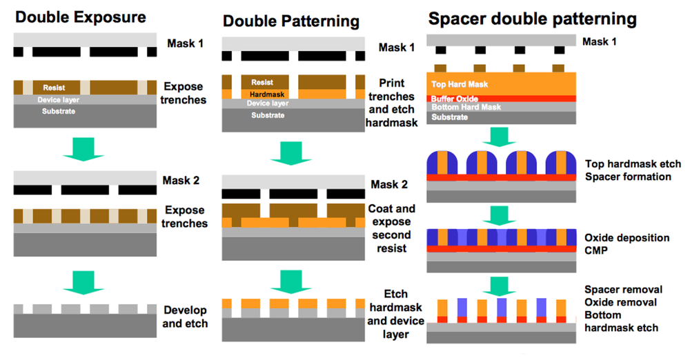
Image The steps for LELE double exposure or patterning and SADP (right) (Source: ITRS)
In this form, the source line, or mandrel, is used for one metal line and metal that fills in between the spacers is used as a second metal line – its course determined by the spacers around surrounding mandrels and not by any features on the mask. The remaining lines can be edited using a cut mask. SADP can involve fewer mask steps than LELELE and, thanks to the accuracy of etch and self-aligned deposition steps – similar to those used to form gates on CMOS transistors – the accuracy of SADP is very high.
Careful choice of layouts makes it possible to define bidirectional features using SADP, although the router needs to take account of the way that every other line’s shape cannot be determined independently – it has to follow the shape of surrounding features that are explicitly defined by the mask. Toshiba showed a technique for this at ASPDAC 2013.
LELE and LELELE processes demand very high accuracy in mask positioning for each pass through the lithography scanner. Practical tolerances are currently on the order of 2nm to 3nm. This restricts the minimum spacing allowed between mask elements and therfore the pitch between on-chip features.
In a 2013 paper looking at the ASIC design problem for sub-20nm processes, Kaushik Vaidyanathan of CMU, with coworkers from CMU and IBM on the joint GRATEdd project, wrote: “Pitch-split double patterning or triple patterning, that is, Litho Etch Litho Etch Litho Etch (LELELE), can print restricted bidirectional patterns at a minimum pitch down to 50nm, sufficient for 14nm node pitch requirements.
“Techniques like sidewall image transfer (SIT) can potentially print bidirectional patterns, with more restrictions, down to a pitch of 40nm, largely accepted to be sufficient for the 10nm node.”
What are the impacts on area and yield?
In principle, the self-aligned techniques can scale further, taking the minimum pitch way below 40nm. But Intel’s head of lithography Yan Borodovsky has warned that each pitch division adds a degree of error to the printed distance between each line. For designers, the chief limitation is on the kinds of features that can be represented using such a process. It becomes increasingly difficult to print any bidirectional features, demanding the use of patterns that are purely unidirectional on a given mask layer. Ideally for lithography, the lines would be straight and of equal width on critical, lower metal layers such as metal one (M1) and metal two (M2) as well as local interconnect and poly.
“Bidirectional-M1 based standard cells have been the preferred choice for decades. However, in the realm of extremely restricted patterning, we observe that the proposed unidirectional-M1 based standard cells have comparable design efficiency, and in most scenarios, superior manufacturability, robustness and scalability compared to bidirectional-M1 cells,” wrote Vaidyanathan et al.
However, when analyzed from a yield-management perspective, the shift to unidirectional or 1D design became less favorable, according to the CMU and IBM team that worked on the GRATEdd project. “We designed a standard cell in the 14nm process based on pure gratings. In line with expectations, the cells turned out to have unacceptably large area. However, surprisingly, the pure gratings-based standard cell did not turn out to be [as] manufacturing-friendly or robust as anticipated.”
The GRATEdd team found grating-based standard cells have thin power-delivery structures that suffer worse electromigration than traditional designs and also have several landing pads of minimum size, which are problematic if successive masks are misaligned.
Image Blocks of patterned M1 layers using bidirectional (left) and unidirectional routing (Source: CMU/IBM GRATEdd)
The team proposed the option of a bidirectional mask design patterned using two orthogonal gratings. In creating the patterning approach, the researchers found that at 14nm, the upper local interconnect layer (CB), which normally runs horizontally was sparse enough to be patterned with less restrictive rules. That change increased the average die efficiency of standard cells by around 10 per cent, slightly compensating for the cell-size growth of a grating-based architecture.
However, by widening power rails to 2x standard width, the researchers found that routability for M2 improved with the use of a unidirectionally routed standard cell, primarily because this type of cell on average provided better access to its I/O pins. Pin access is a key concern for 16nm, 14nm, and 10nm processes (see Guide).
“The advantages of a unidirectional BEOL stack for tight pitch lower metals can’t be over stressed as it drastically reduces litho-hotspots, thereby simplifying ASIC design flow and process ramp, saving design turn-around time,” the GRATEdd authors wrote.
What will be impact on design rules?
Design rules for a process will depend heavily on the precise lithography techniques used for each critical layer, greatly complicating the creation of design rules and ensuring that routers create clean designs. The rules may differ for each layer based on concerns over routeability as well as yield. For example, work performed by ARM and the University of Texas at Austin and presented at ISPD 2014 suggests that standard cells using bidirectional M1 routing with unidirectional M2 provide a better combination of density and cell pin access than a purely unidirectional layout.
The number of last-minute fixes could overwhelm the pre-tapeout DRC process.
Yasmine Badr and coworkers at UCLA proposed in a paper at SPIE Design-Process-Technology Co-optimization for Manufacturability VIII the application of forbidden patterns during layout to reduce the number of fixes needed prior to tapeout. This does not remove all potential bad patterns but does deal with those that either reduce yield significantly or which offer low-routability in the first place and so can easily be switched for more layout-compatible patterns.
The Pattern-DRE software first generates device layers for a library of standard cells and contact locations, feeding that information to a routing-options generator that attempts to work out all of the possible routings – assuming a typical Steiner-tree topology. The tool then checks for forbidden patterns among them – if the routing option contains any of them, it is thrown away.
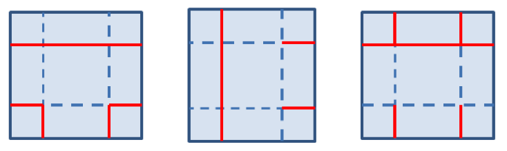
Image Patterns forbidden by SADP because they require a stitch on the long line, but allowed by LELE (Source: Badr et al)
As well as culling forbidden patterns, the tool produces routability metrics for each routing option. The authors wrote: “The reason why we need the number of routing options may not be obvious. While two sets of design rules can produce the same number of routable cells, they actually may not have the same routability-impact. So if prohibiting a set of patterns drastically affects the number of routing options and only leaves a few options, then this means that the set of forbidden patterns has high routability-impact. As a result of eliminating a large number of routing options, there is low chance of a post-route fix for other patterns, that were not forbidden in the design stage.”
Exactly what should be forbidden for a given process will depend on the manufacturing steps. For example, patterns allowed by LELELE will be forbidden for SADP and experience with a process will determine which bad patterns are truly yield-damaging. We can expect that yield data will continue to be mined as has been done with GlobalFoundries DRC+ program to provide IC implementation tools with the information needed to avoid poor yielding structures.
Inverse lithography techniques, which treat the mask design as an inverse mathematical problem that aims at synthesizing an input mask to deliver a desired output pattern on the wafer, may prove valuable in relaxing some of the design rules for SADP and similar lithography processes by making feasible otherwise unprintable designs. However, these techniques are computationally expensive and will involve a tradeoff between CPU time and cost and design-time avoidance of bad patterns.
Patterning decisions could affect designs in more subtle ways. The GRATEdd team suggested that memory designs could change because of highly regular logic layouts. The design rules are making it increasingly difficult to shrink standard SRAM cells and their associated read/write logic. The authors suggested that it may make more sense to synthesise at least the interfaces to each SRAM and incorporate more advanced logic into them to make up for the area increase.
