14nm/16nm processes
Related articles and guides
The 14nm and 16nm processes cover a range of technologies and are designed to succeed the 20nm generation. Most are intended to support finFET or trigate transistor structures, although STMicroelectronics is working on an FD-SOI process that conforms to foundry-class 14nm/16nm design rules.
The processes being prepared by the major pure-play foundries deploy a new generation of finFETs on a routing infrastructure based on that employed by the previous, conventional CMOS 20nm nodes. TSMC has opted for the nomenclature 16nm to describe its finFET-based process, which is consistent with the ITRS naming, while GlobalFoundries and Samsung Electronics use the term 14nm.
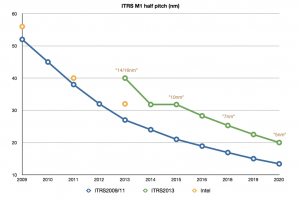
Intel was first to production with a 14nm process that is scaled more in line with older version of the ITRS roadmap – and it will represent the second generation of Intel’s trigate structure.
Image Graph of M1 pitches from current and previous ITRS documents aligned to industry node names
Compared to the 28nm process in mainstream production, 14nm and 16nm present significant challenges to scaling. The continued use of 193nm immersion lithography calls for the use of double patterning on high-density layers, which will increase production cost. Extreme ultraviolet lithography is not expected to be ready for mass production to allow single-mask imaging for this process generation.
Double patterning brings with it associated routing challenges, one of which is more difficult access to standard cell pins because of constraints on interconnect pitch. Tools are beginning to address this issue. (TDF Guide: Cell pin access on 14nm/16nm processes)
Compared to 28nm, increased interconnect resistance will reduce performance (TDF Guide: Interconnect resistance). As well as ‘classical’ reasons for higher resistance, such as the reduced cross-section of the wires, other effects are coming into play. As predicted by the International Technology Roadmap for Semiconductors in 2007, at and below 22nm, carrier scattering, from the boundaries of individual copper crystal grains and the interfaces with barrier layers that separate the conductor from the dielectric, is rapidly pushing up interconnect resistivity and, with it, the resistance of individual wires. By making use of upper, wider metal layers for critical paths, it is possible to recover performance and routers are being changed to allow this use of metal interconnect.
Because of the transition to finFET structures that support higher clock speeds, active power consumption could increase (albeit with higher performance). However, leakage will be improved because of the three-sided gate compared to planar CMOS transistors. The drive to use finFET for performance puts greater emphasis on low-power techniques, such as multibit merging and activity- or transition-conscious design, as well as power signoff to ensure that the onchip power suppy is able to meet peak demands.
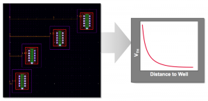
Image Well edge proximity's impact on threshold voltage is a layout dependent effect (Source: Cadence)
As with 20nm processes, the 14nm/16nm generation suffers from layout-dependent effects, largely due to stress, that see isolated transistors exhibit worse performance than those in the centre of a cluster. Although the individual sources of variation may be different to those affecting planar CMOS, there are solutions. They may use simulation and prediction to guide the movement of critical transistors into more benign locations.


