Implementation of a DFM checker for 65nm and beyond
Design for manufacturing (DFM) sign-off is a required step in most deep sub-micron technology design environments. However, there is no common methodology for DFM sign-off. We believe DFM should not only give an estimate of the yield, but should also point out where failures are most likely to occur, and where designers can improve their designs by way of improved CMP, more faithful lithography, higher predictability and the reduction of random defects due to particles.
To this end, a DFM checker based on the Mentor Graphics Calibre YieldAssist and YieldServer tools has been successfully implemented by the Crolles2 Alliance, the European process R&D group made up of Freescale Semiconductor, NXP Semiconductors and STMicroelectronics.
Each DFM guideline within the checker contains recommended values, measurement and scoring metrics, and an associated criticality. Together, these determine global and specific scores calculated by Calibre. The DFM checker is implemented in the TCL Verification Language (TVF) and shares common TVF libraries with DRC and LVS. Results are displayed in Calibre RVE in a user-friendly way. The designer works to improve the lowest-score areas of the design or to address systematic issues related to its physical implementation. The next step consists of more model-based checks, LFD, CAA, and/or equation-based DRC.
Design for manufacturing (DFM) has always been a consideration for designers. When implementing complex designs, they obviously do not want to see them returned by the manufacturing team and, indeed, they really hope that their work will achieve high yields. ‘First-Time-Success’ is the goal. But ‘hope’ is not enough. The designer should be able to judge the quality of the design imple-mentation not only in terms of area and performance, but also in terms of yield, predictability, OPC suitability and CMP compliance. Thus, we need a DFM tool that provides necessary quantitative information about the impact of any trade-offs that are made.
The Crolles2 Alliance has a long history of developing DFM solutions. It previously supported the DFM Point Solution (DPS), which was used until the 90nm node. However for 65nm and 45nm CMOS, the need has arisen for a tool based on DFM guidelines that are aligned with the design rule manual (DRM) specification, and with a formal metrics methodology.
Using Mentor Graphics’ Calibre suite – especially recent improve-ments in DFM functionality – the alliance has built a DFM sign-off tool that has been fully integrated in its CAD flow, with enhanced capability for analysis, development and qualification. This article concentrates on the development of a DFM checker.
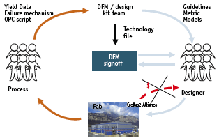
Figure 1. DFM signoff usage
It has become mandatory to apply this tool at each step in the design flow. The results it provides can be used for various purposes. These include DFM-driven placement, the evaluation of auto-fix CAD tools, and the qualification of intellectual property.
The DFM checker is a rule-based tool. It is aimed at reducing the cycle time from design to manufacturing and at increasing the feedback from manufacturing to design (Figure 1).
DFM methodology
DFM is based on continuous improvement. It helps designers make engineering choices to maximize the manufacturability of their products. Adhering to DFM guidelines has obvious benefits. Such practices lead to reductions in yield loss during CMP, reductions in device variability, reductions in sensitivity to random particulate defects, and improvements in OPC cycle time. However DFM can extract a cost in terms of chip area and performance.
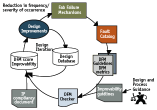
Figure 2. DFM methodology
The specific requirements of a DFM strategy depend on the end-application for the silicon. For example, products for the automotive market should have very high DFM compliance even if this means that the size of the chip increases. However, products targeted at markets such as cell phones and those for many other types of consumer electronics device typically require designers to aim for the minimum chip area. In all such cases, a method of scoring relevantDFM compliance is required.
Figure 2 depicts the DFM methodology defined by the Crolles2 Alliance. First, manufacturing failure mechanisms are analyzed. Then, a fault catalog is created explaining all the defect mechanisms encountered in available products or test chips. Based on the fault catalog, DFM guidelines and metrics, specification documents are written. These documents, together with improvability guidelines, are then used to develop a DFM checker.
Each DFM guideline refers to a DFM metric. The designer uses the DFM checker to measure the quality of the design and analyze local improvement opportunities, which we term ‘Low Hanging Fruit’ (i.e., DFM violations that can be fixed without requiring large-scale changes to the layout). The designer must respect score thresholds given in the IP compliance document. Fixes can be made by hand, or by using automatic fixes available in CAD tools. These tools are evaluated and benchmarked using the DFM checker. This cycle should lead to a reduction of the frequency and severity of failures.
DFM metrics and guidelines
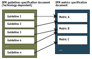
Figure 3. DFM guidelines and DFM metrics specification documents
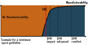
Figure 4. Manufacturability
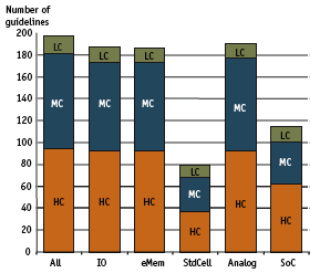
Figure 5. Number of CMOS 045 DFM guidelines per application criticality
DFM guidelines
DFM guidelines are recommended rules. Unlike DRC rules, there is no obligation to fix all violations of the DFM guidelines. Some of the DFM guidelines are rules that already exist in the DRC checker. For these rules, the first step away from the DRC value yields the largest benefit in terms of manufacturability improvement. Figure 3 shows the binning approach defined for DFM guidelines.
For each guideline, several values are defined. The first overall value is the ‘DRC value’. The layout must be at or beyond this value. ‘DFM impact’ is the first DFM value, for which the impact on the manufacturability
is expected to be the highest. ‘DFM comfort’ is the last DFM value – no further improvement is expected (Figure 4).
DFM guidelines are divided into several subsets for each target design category (Figure 5, p36). We selected five categories of design: analog, embedded memory (eMem), IO, standard cell (StdCell) and system-on-chip (SoC). Since not all DFM guidelines have the same impact on the manufacturability, a criticality is defined for each DFM guideline. We have three categories of criticality: High-Critical (HC), Medium-Critical (MC) and Low-Critical (LC).
Each DFM guideline is defined to improve the layout in terms of one or more potential manufacturing issues. Our experience has confirmed that optimizing some DFM rules can have a negative impact on others. A well-known example concerns via redundancy and spacing. When you double vias, you are more likely to create spacing violations, increasing the risk of random particulate defects. If you apply different weights for these two issues, you will favor one failure mechanism over the other. If you assign the same weight to both mechanisms, you might not be able to find an improvement for either one.
Another example is seen with wire spreading when it is carried out by auto-fixes in CAD tools. If the spreading is not done carefully, it is likely to create jogs, and this will have an impact on OPC.
To address these limitations, we first developed metric and scoring systems that measure respectively the quantity of violations for one guideline or a group of guidelines. Then we created guidelines for each DFM group (Figure 6, p36). The designer can then monitor the scores across these five groups, in order to get the best trade-off and DFM optimization for the target market.
DFM metrics
Any DFM methodology requires the definition of metrics, and those metrics should not necessarily be linked solely to the yield simulation. They should reflect the manufacturability for issues such as OPC sensitivity, sensitivity to random particulate defects, and/or SPICE model sensitivity.
A DFM metric is a mechanism for quantifying the DFM violation attached to each guideline. For instance, for a minimum space guideline, the attached metric is the length along which the minimum spacing constraint is violated. For a redundancy guideline, the metric is the count of configurations with single vias. The metric defined can be measured using functions within Calibre YieldAssist. In order to be able to compare metric results for different guidelines, we normalize area, length and count to the same units. We do this by dividing the metric result by a technology dependent reference value (1).
For area: metric = area / reference area (1a)
For length: metric = length / reference length (1b)
For count: metric = count (1c)
Figure 6. Correlation of DFM scores to thresholds
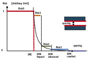
Figure 7. Risk – example for a minimum spacing guideline
For each guideline, we define the DFM value (from ‘DFM impact’ to ‘DFM comfort) and a criticality (LC, MC, or HC). From these two factors we derive the Weighted DFM metric, WDMi (2).
WDMi = Risk x CriticalityFactor x Metric (2)
The criticality factor is a scalar value associated with each criticality level. The risk is calculated as a function of the DFM value of the guideline considered, and should reflect a yield model. Figure 7 represents the risk associated with a minimum spacing guideline.
For guidelines related to discrete (i.e., non-continuous) phenomena, the risk is a function of the interval where the rule value is located. For a guideline related to continuous phenomena (e.g., a minimum spacing), the value of the risk is interpolated between each interval.
Scoring system
Once a weighted metric is calculated for each DFM guideline, we are able to determine a global DFM score by combining these metrics together. Such a score is needed for different applications, as noted earlier. A straightforward method of defining a global DFM score is to take the average of all the metrics. We call this global score the Weighted DFM Metric (WDM) (3). Even though such a score may be useful, for instance to measure the improvements made to one design, it does not fit with all the application needs. Therefore, we have defined two additional scores: the Manufacturing Index (MRx) (4), and the Normalized DFM Score (NDS) (5).
![]()
The manufacturing index (MRx) is the application of a yield formula, such as the Poisson function, to the average of all metrics. It gives us the raw quantity of DFM violations. It has the advantage of being a value between 0 and 100%, which is easy to understand. However, such a score does not allow us to, compare two designs of different sizes or different functionality.
![]()
The Normalized DFM Score is a score normalized by a value, the ‘Normalizer’. The Normalizer is chosen to be representative of the design and is calibrated to have a resulting score of 75% on a Crolles2 process reference test chip. Different choices can be adapted for the Normalizer.
![]()
Implementation for Calibre
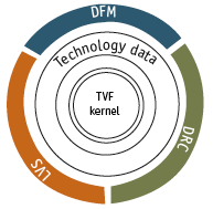
Figure 8. TVF platforms
TVF platform
The implementation of the DFM checker was achieved using a strategy that heretofore has not been used for Calibre DRC and LVS. The approach is based on the TCL Verification Language (TVF). This is a superset of TCL that is embedded in Calibre. TCL has the advantage of being easy to learn, and thus allows the development of common procedures that can be shared between verification modules and between technologies. Based on the DFM development, DRC and LVS are now being ported to TVF. Therefore the DFM checker shares a common TVF platform with DRC and LVS and has been developed for the 65nm and 45nm nodes.
The TVF platform is organized in three layers (Figure 8). The TVF kernel regroups all low-level procedures: such as technology data parsing, handling of user options, and database management. Technology data groups process information into associated text files: electronic guidelines, DRM, layer list, etc. Finally, in the DFM, DRC, and LVS modules, verification procedures are implemented. Each of these three modules can use verification procedures defined in the other modules. The TVF platform is very efficient, since it permits a high level of reusability across technologies. Indeed, the DFM checkers for 65nm and 45nm share more than 80% of their TVF code.
Calibre DFM function usage
The DFM metrics have been implemented using the DFM functions available in Calibre 2006.4.
For the DFM metric calculation (Figure 9):
‘DFM PROPERTY’ clusters edges or polygons together, and calculates
‘AREA’, ‘LENGTH’, ‘COUNT’, ‘RUNLENGTH’, and ‘SPACING’;
‘DFM FUNCTION’ is a user-defined mathematical function;
‘DFM ANALYSE’ gives a result for the total chip, by window or by cell;
‘DFM RDB’ outputs a violation, with its metric value in a .rdb text database, or in a YieldServer database.
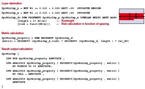
Figure 9. DFM metric calculation with Calibre
Using these functions, we can calculate the weighted metrics for eachguideline (i.e. the risk and the metric value) to output metrics for the chip by window or by cell, and to calculate the global scores (WDM, MRx and NDS) for the chip by window or by cell.
The DFM checker makes intensive use of ‘DFM PROPERTY’. This function clusters polygons and edges together and attaches a property value that can be reused in a different DFM expression.
All the DFM metrics and the score are saved in a DFM database, a new binary format defined by Mentor Graphics that can be accessed by Yield Server and Calibre DFM RVE. All metrics are annotated using the ‘ANNOTATE’ keyword. These annotations specify the categories and the type of the rule, the binning, the type of analysis and so on. Calibre RVE is able to retrieve these annotations for display in the DFM report card.
DFM results analysis
Calibre RVE opens the DFM database (dfmdb) directly. Metrics and the score are displayed in a DFM report card. Within the DFM report card, we are able to sort the metric results and to display the violations associated to each guideline in a flat or hierarchical mode. We can also filter the guidelines by DFM group, as defined in Figure 6. The results by window or by cell are also accessible.
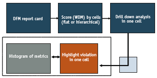
Figure 10. Flow for analysis by cell
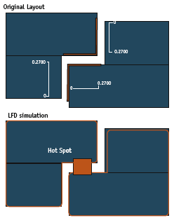
Figure 11. LFD simulation
We show in Figure 10 (p.38) the flow for the analysis of guidelines by cell. In more specific terms, however, from the ‘rule summary’ tab, we get the global score for each cell. For example, we can select a cell having the highest weighted metric (WDM) and drill down to display the guidelines violated in this cell. From the ‘drill-down’ table, we can display the violations in a layout viewer. On screen during use, the violations will appear colored as a function of their metric value: a property is attached to each violation that is equal to the metric value. We may also display the histogram corresponding to the metric binning for the corresponding guidelines.
To analyze the DFM score by window, the layout is divided in a certain number of windows that have the same size. Metrics and scores are calculated for each of these windows. The flow is the same as for the cell analysis. First, we display the global score for each window. Then, we can drill down within a particular window and display the DFM guidelines violated there. From the ‘drill down’ tab, we can display the violation in the layout viewer. We have a further option with this kind of analysis in that we can display the window color map of metric and score. This is especially interesting for guidelines linked to the design’s sensitivity to random particulate defects. In such cases, we need to avoid hot spots with a high concentration of violations. These increase the risk of a failure in the circuit.
Model-based usage
For the 65nm and 45nm nodes, the traditional rule-based approach of physical verification no longer enables us to check designs against complex process requirements. Indeed, for some cases where there are dense-end-of-line or parallel run-length issues, DRC or DFM analysis gives no results, although these configurations may be at risk due to lithography variations.
A methodology for addressing such requirements has been implemented by the Crolles2 Alliance. It is based on usage of the LFD kit that is available for the 65nm and 45nm nodes.
First, the rules described in the design rule manual or DFM guidelines are implemented in a constrained way. The second step consists of running DRC or DFM analysis on standard cell blocks in order to get a significant number of configurations, many of which may actually be fake errors. Then the Crolles2 Calibre LFD kit is run, in order to differentiate between the true and fake errors. Finally the description of the rule is refined in the DRM or guideline and delivered along with an updated DRC or DFM implementation. Figure 11 shows an example of an LFD simulation done to refine complex minimum spacing rules between thick metals when the run-length between the metals is greater than a minimum value.
Using the ‘DFM PROPERTY’ function, we are able to define equations for a DRC or DFM rule in order to have an implementation that will cover most hot spots found by LFD. However, our experience with 45nm CMOS design and test chips shows that a DRC or DFM implementation that catches all lithography hot spots becomes more and more complicated to achieve. Therefore, the LFD kit is now part of our DFM sign-off platform.
Application
The DFM checker has multiple use models. It should be used in a DFM sign-off flow to get the DFM scores for a design and to validate its DFM compliance. The defined DFM metric scoring allows us to decide on a score threshold and our normalized DFM score is calibrated to the process test chip. The DFM checker is also used to validate auto-fix CAD tools and it will be used for DFM-driven synthesis. Then it is used to optimize layouts by hand.
An important feature in development aims to enable us to catch areas where local improvements can be made without creating DRC violations. This feature is called ‘improvability’. It will not replace auto-fix tools but should allow designers to address ‘Low Hanging Fruit’ issues with greater ease, and without large-scale modification to the original design.
Freescale Semiconductor
6501 William Cannon Drive West
Austin
TX 78735
T: 1 800 521 6274
W: www.freescale.com
STMicroelectronics
39, Chemin du Champ des Filles
C. P. 21
CH 1228 Plan-Les-Ouates USA
Geneva
Switzerland
T: +41 22 929 29 29
W: www.st.com
NXP Semiconductors
Postbus 90050
5600 PB
Eindhoven
The Netherlands
W: www.nxp.com
