Verifying low-power intent in mixed-signal design
An exclusive extract from Cadence Design Systems’ Mixed-Signal Methodology Guide provides an excellent overview of its discrete topic and a flavor of the book as a whole.
Mixed-Signal Methodology Guide
The Mixed-Signal Methodology Guide: Advanced Methodology for AMS IP and SoC Design, Verification and Implmentation was published by Cadence Design Systems this Summer.
It provides a broad but also, where necessary, deep overview of the techniques needed to address today’s mixed-signal designs. The authors have tailored it to serve as a reference for a catholic readership of analog, digital and mixed-signal designers, as well as verification and physical implementation engineers and managers.
This exclusive extract from Chapter 4, “Mixed-Signal Verification Methodology”, specifically addresses the challenges presented by verifying intent for low power, a subject of ever increasing importance, and gives a good flavor of how the Mixed-Signal Methodology Guide has been well pitched at its wide target market.
The book is now available for purchase on both Lulu and Amazon.
Introduction to low power
The modern day SoC is almost always a complex mixed-signal system. The verification of such a system requires careful planning and execution not only in the digital and analog sub systems separately, but in an integrated fashion where relationships between the digital and analog functionalities in the SoC are taken into account.
In the previous generation of verification planning, it was common practice to create a detailed plan and specification goals of the digital islands of an SoC, and then approximate the analog functionalities of the chip by assuming simple discretized models of the analog blocks. You thereby created a convenient system where the analog parts of the chip could participate in the overall verification process by essentially appearing as a digital approximation. However, the systems of today can rarely be approximated to this level of simplification without sacrificing a significant part of the verification goals.
It is now common for the digital and analog subsystems to have multiple feedback paths and complex relationships with each other. To accurately verify such systems, it is imperative that the verification planning and execution process involves both analog and digital as integral parts of the system. A central aspect of this approach is to define and apply traditional verification methodologies to analog and mixed-signal parts of the design without sacrificing the accuracy of the analog design blocks.
Low power is one of the more crucial aspects of verification of an SoC at this time – if not the most crucial. With the introduction of analog functionality in the system, the process becomes even more complex, since verification planning now must include analog and digital interactions in addition to defining power verification goals on the digital blocks of the chip. Consequently, mixed-signal modeling and simulation tools need to evolve to meet these requirements of functional verification. This extract describes this evolution first by introducing some common low-power related concepts, followed by a detailed account of the low-power aware value conversion process across A/D boundaries.
Mixed-signal low-power verification techniques will be applied to a complete design, and metric-driven methodologies, such as assertions, will be extended to mixed-signal designs. These techniques can be combined with power-aware modeling to deliver significant value to the mixed-signal low-power verification process.
In this book, Common Power Format (CPF) has been chosen to be the vehicle to express power intent.
Review of basic low-power features
This section explains some basic power intent concepts, not necessarily in the context of mixed-signal designs. This will establish the background for the reader to understand the mixed-signal aspects of these concepts when they are elaborated.
Power Domain
A power domain is an abstraction for a collection of instances that use the same power distribution network during normal operation and that either can be simultaneously switched on or off, or treated as always on.
Power domain example in CPF:
create_power_domain -name Pd_A \
   -shutoff_condition {pm_a} \
   -active_state_conditions \
                  {low@!pmc.pw_stdby_pd \
                  high@!pmc.pw_awake_pd} \
   -instance inst_A
The power domain called Pd_A has been created and instance inst_A has been associated with this power domain. Also, conditions have been specified to indicate when this power domain would go into shut-off mode and what conditions would drive this power domain to go to the nominal conditions called low and high.
Isolation
Isolation logic is typically used at the output of a powered-down block to prevent floating, unpowered signals (represented by unknown or X in digital simulation) from propagating out of powered-down blocks. The outputs of blocks being powered down need to be isolated before power can be switched off and they need to remain isolated until after the block has been fully powered up. Isolation cells are placed between two power domains and are typically connected from domains powered-off to domains that are still powered-up.
In some cases, isolation cells may need to be placed at the block inputs to prevent an electrical connection to powered-down logic. If the driving domain can be off when the receiving domain is on, the receiving domain needs to be protected by isolation cells. The isolation cells may be located in the driving domain, or they may be in the receiving domain.
Example of isolation rule specification in CPF:
create_isolation_rule -name iso1 \
   -isolation_condition pm_iso \
   -from Pd_A -to Pd_B \
   -isolation_output hold
State Retention
When a power domain is powered down, the states of certain sequential elements (registers, latches, flip-flops) in the power domain may be saved and retained for the entire shutoff period, to enable faster recovery on restoration of power. The states will be restored to the values before shut-off to accelerate the power-up process. These sequential elements can be implemented by special state retention cells.
Example of state retention rule specification in CPF:
create_state_retention_rule \
   -name SR1 -domain Pd_A \
   -restore_edge pm_sr_a
Nominal condition
A nominal condition is a typical operating condition under which the design or blocks perform. An operating condition is determined by the voltages of all power supplies associated with a power domain, including the power voltage, ground voltage and optionally the body bias voltage for PMOS and NMOS transistors. Each nominal condition must also be specified with a state which can be on, off or standby.
Example of nominal condition specification in CPF:
create_nominal_condition -name high \
   -voltage 1.8 -state on
create_nominal_condition -name low \
   -voltage 1.2 -state standby
create_nominal_condition -name off \
   -voltage 0.0 -state off
Power mode
A power mode defines the state of the nominal conditions of all power domains in a specified scope of the design. In other words, a power mode is a collection of power domains, each of which operates at a specific nominal condition. Power modes enable the identification of which combinations of power domain states are valid, and which are not. Any combination of nominal conditions that is not defined in the low-power specification should be considered an illegal power mode.
Example of power mode specification in CPF:
create_power_mode -name ModeD \
-domain_conditions {PD1@high PD2@high} -default
create_power_mode -name Mode1 \
-domain_conditions {PD1@low PD2@high } QUERY SPACE BEFORE LAST BRACKET
create_power_mode -name Mode2 \
-domain_conditions {PD1@low PD2@low
Power shut-off
Power shut-off is the technique to turn off power supply to parts of a chip. Prior to shutting down power to a block, the signals connected to the affected block must be isolated and key states may be retained so that power up sequences can be optimized. This is shown in Figure 1. When performing functional verification on a mixed-signal chip where parts of the chip go through a power-up and power-down sequence, the electrical voltage corresponding to a digital driver must be specified so that a powered-down state can be correctly represented on the analog side. More details on power shut-off voltage will be explained in the succeeding sections.
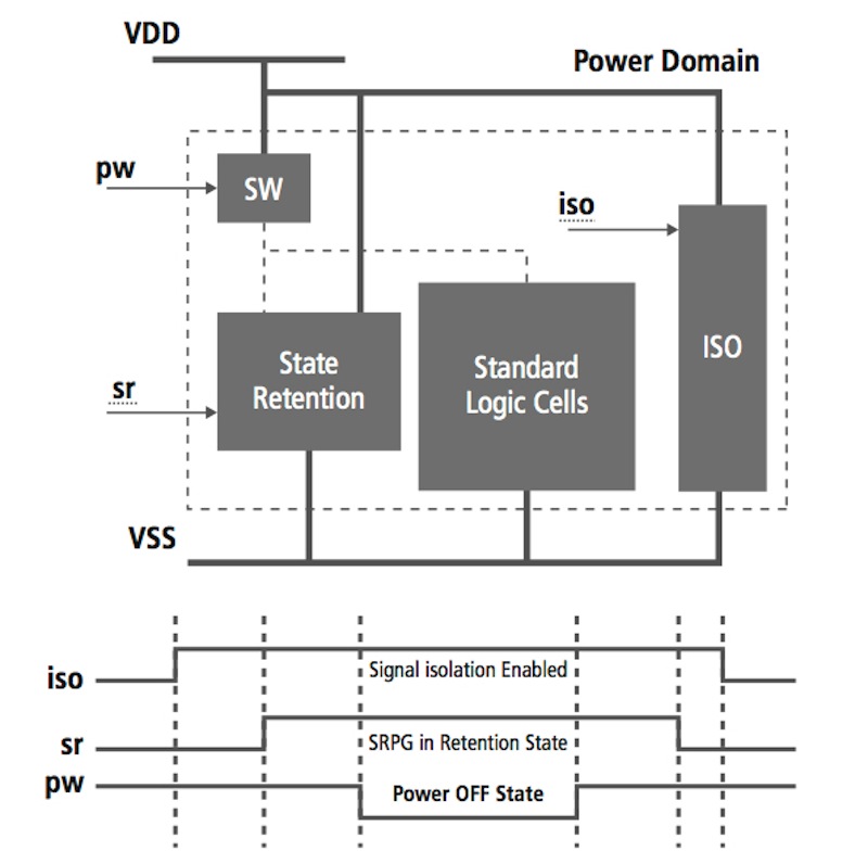
Figure 1
Illustration of power-up and power-down sequence (Source: Cadence/Mixed-Signal Methodology Guide – click image to enlarge)
Multiple supply voltages
Assigning different power domains with different supply voltages is a common technique to achieve trade-off between power consumption and performance requirements.
There are three power domains in the example design in Figure 2, each at a different voltage level (PD1 at 0.8V, PD2 at 1.2V and PD3 at 1.8V). Note the presence of level shifters between the power domains so that signals can pass from one domain to another across different voltage levels.
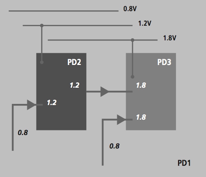
Figure 2
Schematic diagram of multiple power domains (Source: Cadence/Mixed-Signal Methodology Guide – click image to enlarge)
Low power in mixed-signal
A mixed-signal design integrates both analog and digital functionality on the same chip. The interaction between an analog and digital subsystem is central to how a mixed-signal design works. When such interaction is manifested in the form of signals passing across the analog and digital domain boundary, the signal value must be converted and this is achieved by inserting logic-to-electrical and electrical-to-logic connect modules.
In a power aware mixed-signal simulation, it is common for a block in a discrete domain with power intent specified on the block using CPF to connect to another block belonging to the continuous domain. In such a situation, the process of logic-to-electrical or electrical-to-logic value conversion must take the power intent aspect into account. It is against this background that power-aware value conversion aspects and requirements of mixed-signal simulators are introduced and now being implemented by vendors.
In order to explain the role of a power-aware value conversion, consider Figure 3.
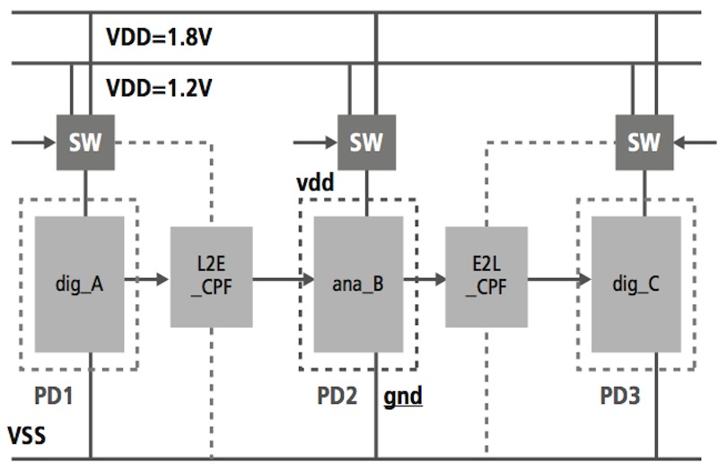
Figure 3
A mixed-signal design with power domains (Source: Cadence/Mixed-Signal Methodology Guide – click image to enlarge)
Digital block dig_A belongs to the power domain named PD1 and is driving an analog block called ana_B which belongs to power domain PD2. This analog block in turn is driving another digital block called dig_C that belongs to power domain PD3. Note also that all three power domains have two operating voltages – one at 1.8V and the other at 1.2V.
Logic-to-electrical conversion
The power-aware logic to electrical conversion module, denoted by L2E in Figure 4, is responsible for reading a logic signal and its associated power domain information, and then producing the appropriate electrical voltage at the output.
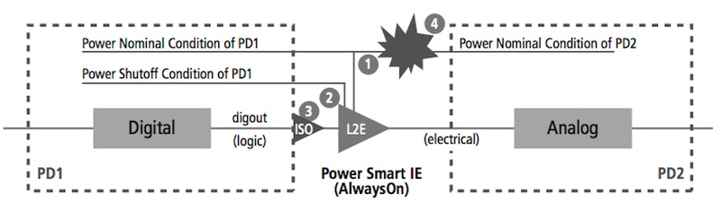
Figure 4
A Power-aware logic-to-electrical conversion module (Source: Cadence/Mixed-Signal Methodology Guide – click image to enlarge)
The conversion process involves the following:
- Conversion of the four-state logic to the corresponding electrical voltage values as specified by rules defined in the conversion module. In one leading mixed-signal simulator, the automatically inserted logic-to-electrical connect modules implemented using standard Verilog-AMS language provide these values as user customizable module parameters.
- Detection of the shut-off condition of the
PD1power domain and thereby differentiation between an unknown state (X) arising from power shut-off as opposed to a functional X-state. In case of the former, the user may wish to specify a certain electrical voltage, or a range of voltage values, to be able to differentiate between the electrical representation of power shut-off state vs. that of functional X-state. [Refer to (1) in Figure 4] - Detection of the nominal condition of a power domain and the voltage value associated with that nominal condition. As an example, if the power domain
PD1in Figure 4 has a nominal condition associated with it calledhigh, then a logic net residing inPD1and carrying value1’b1will represent an electrical voltage of 1.2V at the output of the logic to electrical connect module. - Linkage of the supply voltage of the conversion module
L2Ewith the power domain of the digital instancePD1. - Performance of a dynamic check with the simulator ensure that the supply voltage of the conversion module is consistent with the nominal condition of
PD2and may wish to notify the user during simulation as and when such violations occur. [Refer to (4) in Figure 4]
Figure 5 provides a pictorial representation of a power-aware logic to electrical value conversion process as the power domain transitions from a 1.8V nominal condition to a 3.3V nominal condition before turning to a shut-off state.
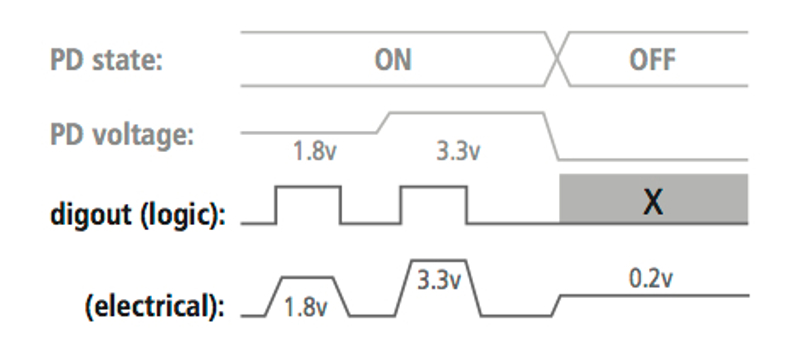
Figure 5
Power-aware logic-to-electrical conversion (Source: Cadence/Mixed-Signal Methodology Guide – click image to enlarge)
Electrical-to-logic conversion
The fundamental premise behind the need for a power-aware electrical to logic conversion is the fact that an analog instance, whose behavior is expressed and simulated in the continuous domain, can also reside in a switchable power domain. This is most commonly seen when the user decides to switch the abstraction of a block, residing in a power domain PD1, from a digital model to an analog one, for reasons such as higher accuracy or measurement of performance characteristics. If the output from such a block is driving a digital instance residing in a power domain PD2, then the expectation is that the behavior of the input to the digital block would be consistent regardless of whether the block was implemented in analog or digital.
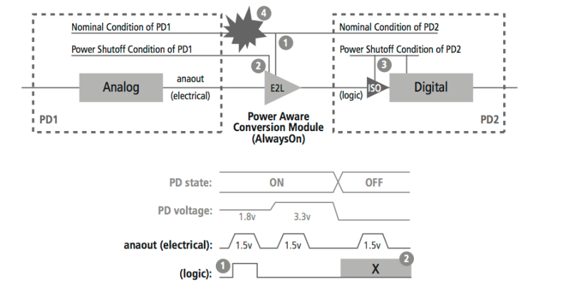
Figure 6
Power-aware electrical-to-logic conversion (Source: Cadence/Mixed-Signal Methodology Guide – click image to enlarge)
The following factors need to be noted when performing an electrical to logic value conversion in a power-aware fashion.
- The supply voltage of the conversion module must be linked with the working voltage of the power domain the digital instance resides in [Refer to (1) in Figure 6].
- The logic output will go to an X state when
PD1is in shut-off [Refer to (2) in Figure 6]. - An isolation device needs to be placed at the input of the digital receiver in order to prevent propagation of unknown values from the off domain to the on domain [Refer to (3) in Figure 6].
- If the driving and receiving power domains have different nominal voltage conditions, it must be treated as an error condition and the power intent specification must be checked as this would otherwise result in electrically inconsistent behavior [Refer to (4) in Figure 6].
The techniques adopted for logic to electrical and electrical to logic conversion described here also apply to bi-directional logic and electrical conversion where both input and output of the conversion module can act either as a driver or a receiver.
Controlling the analog power supply with low-power specification
It is quite common in mixed-signal verification to switch the representation of a module from digital to analog or vice versa. To run such mixed-signal simulation, an analog voltage source for the power supply will typically be provided. In cases where part of the mixed-signal system is designed with power awareness specified using, say, CPF, the voltage source becomes a part of design function. The power supply to analog blocks, even for a functional verification, needs to be defined in a way consistent with the system-wide power intent.
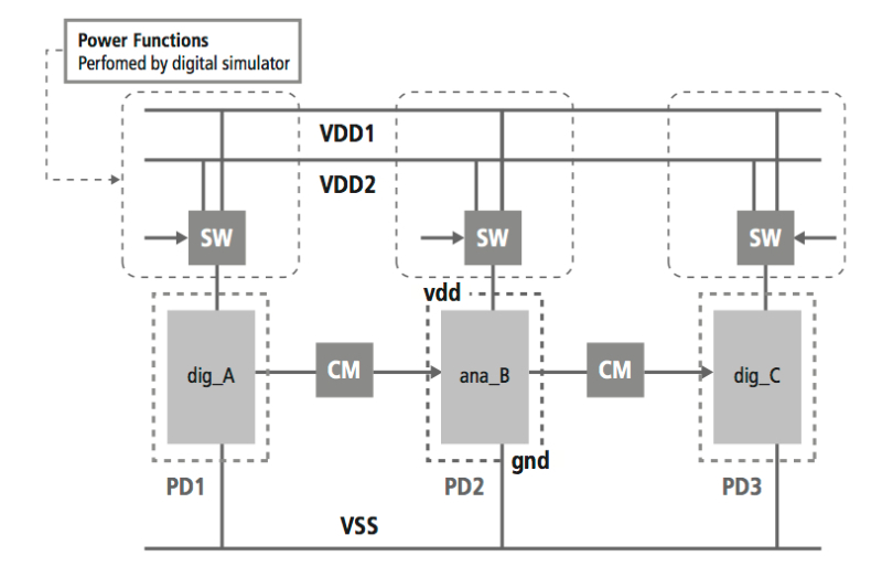
Figure 7
Controlling voltage supply with Common Power Format (CPF) (Source: Cadence/Mixed-Signal Methodology Guide – click image to enlarge)
In Figure 7, the digital blocks, dig_A and dig_C, are represented in Verilog, and their power behavior is defined using CPF. Assume that the analog block ana_B also has some low-power characteristics and that the power behavior is expressed in the same format as the digital blocks. The code snippet below shows how the user specifies a power and ground connection for the ana_B block that would be used when ana_B is represented as an analog component, possibly as a SPICE netlist or a schematic. The functional verification tool can synthesize a power supply model in accordance with the power domain specification of the block ana_B and then make a virtual connection of the power supply model to the power connection of ana_B, thereby simulating the effect of power domain specification – using the same language that is being used for pure digital blocks elsewhere – on the analog blocks.
Specification for power and ground pins in CPF:
# Power Domain
create_power_domain -name PD2 -instances {ana_B} - shutoff_condition pso1

# Specify global power supply and ground
update_power_domain -name PD2 \
   -primary_power_net vdd -primary_ground_net gnd
The block ana_B belongs to a power domain PD2. When ana_B is changed to an analog representation, such as a SPICE sub-circuit with power supply port vdd and ground port gnd, the functional verification process will continue to work applying the same power supply characteristics as laid out in the specification of power domain PD2 to the analog block ana_B.
About the authors
Prabal Bhattacharya has a Bachelor of Engineering degree from Jadavpur University in India in Electronics and Telecommunications. He has been working in various groups in Cadence’s Analog and Mixed-Signal simulation solution for the last 15 years and currently holds the title of R&D Architect. His special area of interest includes mixed-signal simulation and verification, compiler techniques for various analog and mixed-signal languages and software architecture and reuse in simulation products.
Don O’Riordan is a Senior Architect for the Cadence Custom IC and Sign-off Division with over 20 years of experience in design and verification within the EDA industry. He has held positions at Silvaco on SPICE Modeling, at Transmeta Corporation on CPU verification, and at Cadence on a variety of design and verification tools including SPICE circuit simulation, AMS mixed signal simulation and debug, and the Virtuoso schematic capture and analysis environments. Don is the holder of seven patents, and a Masters Degree from the National University of Ireland.
More on Mixed Signal Methodology Guide
The home page for the Mixed Signal Methodology Guide provides a full breakdown of chapters and also a link to a further opportunity to preview Chapter 1, “Mixed-Signal Design Trends and Challenges”. As noted earlier, the book is now available for purchase on both Lulu and Amazon.
Contact
Cadence Design Systems
2655 Seely Avenue
San Jose
CA 95134
USA
T: +1 408 943 1234
W: www.cadence.com
