Enabling 3D-IC design
Meeting the challenges of moving beyond planar integration to side by side, and eventually truly stacked, dice, for designers, tool vendors and the supply chain.
As planar integration becomes more complex, integrating IC functions in three dimensions becomes more attractive. Although the tool, packaging and semiconductor industries have some way to go before it is possible to place and route functions arbitrarily on a stack of interconnected die, 2.5D integration, in which dice sit side by side on an interconnecting silicon substrate, can provide useful integration advantages now. Developing a 2.5D-IC design flow and supply chain will also smooth the path to true 3D-IC design and integration.
Early targets for 3D integration
A number of early applications of 3D integration techniques are emerging. In The applications closest to market are:
Memory cubes
Memory cubes are stacks of identical Flash or DRAM die, interconnected vertically using a relatively small number of through-silicon vias (TSVs) to link a die to the one below, without using a redistribution layer (RDL) to reroute the connection points.
In one implementation, eight 2Gbit Flash die were thinned to 50µm each and then stacked to make a 16Gbit device. The resulting device was 30 percent thinner and hads a 15 percent smaller footprint than a wire-bonded equivalent.
Silicon interposer-based 2.5D-ICs
Silicon interposers are single-sided passive interconnection structures built using the upper metal layers of a standard IC process. In a silicon interposer-based 2.5D-IC, active dice are placed on the surface of the interposer and connect to each other through its interconnect scheme using microbumps as shown in Figure 1. TSVs link the interconnected dice through the substrate to solder balls that connect to the interposer’s package, or to an RDL that re-routes the connections to the package.
This approach enables much denser interconnections between dice than would be possible with packaged parts, as well as cutting signal latency and power consumption.
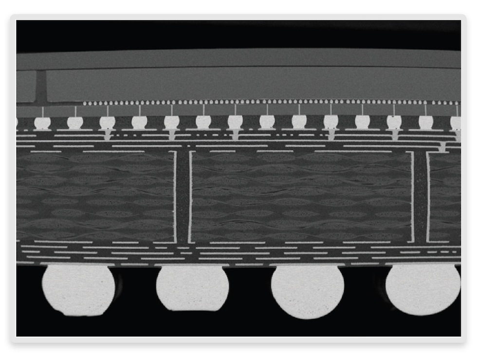
Figure 1 The Xilinx Virtex 7 family uses a silicon interposer built using a 65nm process (Source: Xilinx)
Memory on logic
Integrating memory on top of logic can ease bandwidth bottlenecks. In one approach, ST-Ericsson has built a Wide I/O memory bus in the middle of a processor design, and then stacked a Wide I/O memory cube on it. Integrated thermal sensors help set the refresh rate for the DRAM, to counter its tendency to lose data more quickly as it warms up.
True 3D-IC integration
True 3D integration, in which chip functions can exist on any layer of a stack of die, has yet to be widely demonstrated, in part due to cost, heat management, and supply-chain issues. The cost of making TSVs is still too high for most applications: adding a 5µm diameter, 10:1 aspect ratio ‘via middle’ TSV process to a wafer manufacturing flow is estimated to add $80 to $100, or 2 to 3%, to its production costs. Other key issues include power and heat management, design for test and yield, and the supply chain.
The EDA challenge
Introducing 3D integration, especially true 3D stacks, creates new issues for designers.
For example, introducing TSVs, microbumps, and C4 balls stresses the substrate around them. 3D stacks bring different materials into close contact, where their differing coefficients of thermal expansion can induce stresses in the substrate materials. Both sources of induced stress can lead to silicon deformation, which changes its carrier mobility and so affects transistor performance. Modeling and characterizing these stresses is vital to understanding the effect of 3D integration techniques on device performance and reliability.
Figure 2 shows the impact of TSV-induced stress on a transistor’s ON current (ION). Being able to characterise this impact is vital to knowing how large a keep-out zone to create around the TSV.
Figure 2 TSV stress impact on transistor’s ION (Source: Synopsys)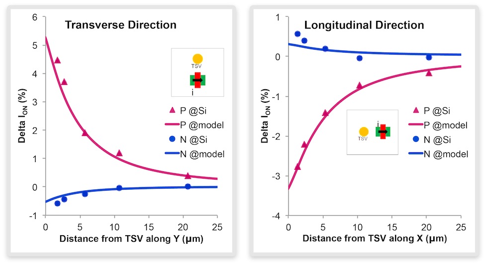
Another key issue to be resolved is that 3D integration usually involves dice built on different process technologies (for example, a 65nm interposer carrying 28-nm dice). Today’s planar IC tools can usually only handle one process technology so static timing analysis, design-rule checking, and layout-versus-schematic tools all need upgrading to support multiple technologies.
An evolutionary approach to 3D integration
Based on the technology trends, their timeline and impact on EDA, the best way to achieve 3D integration at the moment is to use a 2.5D-IC, silicon interposer-based approach that can draw on existing EDA tools. Most of Synopsys’ 2.5D-IC design flow, including standard-cell placement, clock-tree synthesis, routing, optimization and so on, is the same as its advanced 2D design flow. Other parts of the flow have been upgraded, as follows:
Test
Test tools have been upgraded to address 3D-IC designs, combining logic and memory test technologies based on existing standards for core-wrapping (IEEE 1500) and boundary scan test (IEEE 1149.1 and 1149.7). Synopsys is also participating in the IEEE P1687 (a.k.a. IJTAG) standardization effort, which will help organize the stack’s design-for-test (DFT) and design-for-debug (DFD) strategies, out of a mixture of DFT/DFD efforts on each tier.
Synopsys supports the IEEE P1838 standardization effort, aimed at providing test access to TSVs so that tools can find and repair any defective interconnects between bare dice.
Extraction
Extraction tools have been upgraded to account for microbumps, TSVs, C4 bumps, and RDL both on the front and the back of the wafers. Each tier of a stack is extracted separately, including all the 3D structures belonging to it. A hierarchical netlist instantiating all the tiers can be produced for use in electrical simulations.
Synopsys HSpice® and FastSpice tools have been upgraded to understand 3D structures. The models for microbumps, TSVs, C4 bumps, and RDL are regularly updated to reflect an evolving understanding of the process technology-related aspects, as well as the reliability and accuracy requirements.
Physical verification
Synopsys’ physical verification tools have been upgraded to deal with 3D-IC. While it is possible to use 2D tools for 3D designs, it isn’t convenient. 3D structures and rules can be added to a 2D-IC DRC deck, but dealing with the LVS decks, and also manipulating the netlist, is much more difficult.
Place and route
The Synopsys 2.5D-IC silicon interposer-based physical implementation solution uses existing tools. A silicon-interposer can be considered as the top level of a hierarchical design, and the various die as its hierarchical blocks. They can then be routed together using the IC Compiler™ Zroute technology.
Zroute technology has three advantages for routing a silicon interposer:
- It is designed to deal with millions of nets, unlike tools derived from PCB layout.
- It can handle an arbitrary number of layers.
- It can automatically complete the routing of any number of nets and layers.
Synopsys is also developing an RDL router that can route on 45° angles, to complement the Manhattan router in IC Compiler. Figure 12 shows the RDL routing (shown in green) between a TSV and a C4 bump on the back side of the silicon interposer.
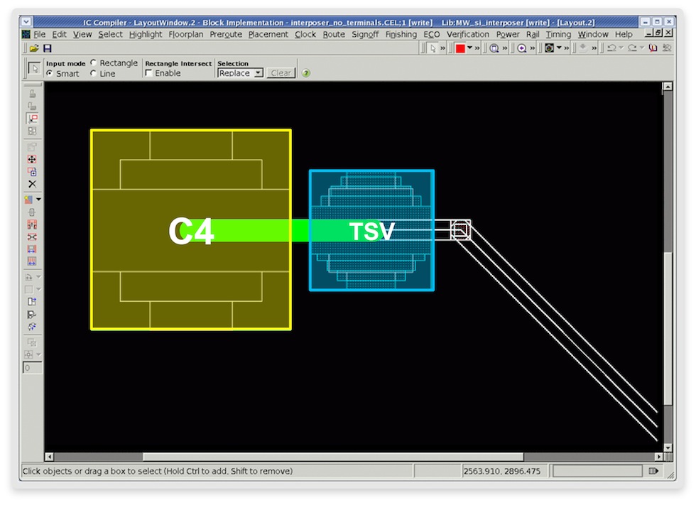
Figure 3 Routing µbump to TSV (top side) to C4 bump (back side) (Source: Synopsys)
The Galaxy Custom Designer tool can also be used to pre-route analog nets. Once the initial floorplanning and the power and ground grid synthesis has been done, Custom Designer can be invoked from within IC Compiler to do net shielding, differential-pair routing, or matched-resistance routing.
Enabling the advantages of 3D
An evolution of existing tools will help make 3D integration, in the form of a 2.5D-IC, silicon interposer-based approach, more widely accessible. Once the basic integration of existing dice is widely understood, the architectural freedom that the third dimension brings can be explored. For example, it would be possible to move the global power and ground mesh for a number of dice onto the silicon interposer, to save die area and enable a simpler manufacturing process. The ability to closely integrate functions should also enable subsystems (memory, logic, analog processing) to be produced on optimised processes, cutting manufacturing costs and improving systemic yield.
The impact of moving to true 3D-IC stacks is more revolutionary. Pathfinding tools may be necessary to deal with the cost, performance, manufacturing, thermal, and test trade-offs, as well as helping to assess whether a 2D or 3D integration scheme is most appropriate.
Author
Michael Jackson is vice president of Physical Implementation R&D at Synopsys. He joined Synopsys in 2002 as part of the Avant! acquisition where he led the engineering efforts for physical design and simulation products. Michael received his Ph.D. in Electrical Engineering and Computer Sciences from the University of California at Berkeley.
This article is based on a presentation given by Dr Jackson at the 2011 3D Architectures for Semiconductor Integration and Packaging Conference.
Company
Synopsys700 East Middlefield Road
Mountain View, CA 94043
Phone: (650) 584-5000 or
(800) 541-7737
