IEDM shows progress on embedded eMRAM
Embedded magnetic RAM is emerging as a contender for on-chip memory not just from a density standpoint but from that of power. In his presentation during the plenary at this year’s International Electron Device Meeting, Samsung Foundry head ES Jung argued the energy usage of eMRAM makes it a better choice than traditional SRAM for densities above 10Mbyte.
Non-volatility makes it possible to power down entire pages of memory when not in use instead of having to keep a current, albeit small, circulating constantly through the bitcells. By the time you get to 1Gbit of memory, eMRAM consumes just 0.5 per cent the power of a comparable SRAM core, Jung claimed. However, endurance remains a potential issue. SRAM has practically unlimited endurance but eMRAM at Samsung can survive around a 10 billion write cycles with ten-year retention at an operating temperature of 85°C.
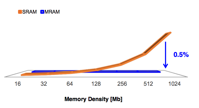
Image Samsung estimates for power differences of SRAM vs MRAM
A number of technical papers focused on eMRAM’s potential for integration into both mature and leading-edge nodes. Imec’s Sushil Sakhare described how the research institute has looked into the PPA comparisons between SRAM and eMRAM to determine how easily spin-torque transfer MRAM – currently the leading contender – can integrate into the future 5nm node processes. One key potential advantage for eMRAM even at that node is that it can be realized using single-patterning with 193nm lithography.
In terms of energy benefit, the crossover compared to regular scratchpad SRAM was 0.4Mbyte, increasing to 5Mbyte for last-level cache (LLC) applications. The Imec team found there is a strong sensitivity for eMRAM manufacturability and density to the underlying contacted poly pitch and its relationship to the metal pitch. A more relaxed bitcell size, tuned to be 2x the contacted poly pitch looks to be the best option for layout to get a circular pillar for the core STT-MRAM element.
Experiments demonstrated it should be possible to hit read and write times of less than 2.5ns and 7.5ns, respectively, for eMRAM, making it a reasonable contender for last-level on-chip cache in computers.
Process choices
Samsung engineers described how they had put an 8Mb STT-MRAM core into a 28nm FD-SOI process aimed at low-power embedded systems, and how it is possible to tune retention against endurance as well as improve overall efficiency to increase both as techniques mature. A GlobalFoundries team also looked at FD-SOI integration, choosing their 22nm version as the target although they said they expect scaling to the 14nm design rules to cut the bitcell area by half. With the aim of putting the technology into automotive controllers, the team said retention could hit the Auto-G1 requirements. Endurance was tested up to a million write cycles.
At Intel, worked shown at IEDM focused on the existing 22nm finFET node, with applications in mobile communications. Their work demonstrated ten-year retention at temperatures up to 200°C but with endurance topping out at around a million write cycles.
To try to push up endurance, a team from Tohoku University and Tokyo Electron concentrated on the process used to create the magnetic tunnel junction, and reducing the amount of damage it has to sustain during production. This low-damage process demonstrated improvements in tunneling magnetoresistance, thermal stability and switching efficiency. The resulting macro, for a 14nm process, pushed endurance higher than 10 billion write cycles and demonstrated ten-year endurance at 85°C.
