SNUG 2016: Intel, TSMC, GloFo back post-finFET research at UC Berkeley
Intel and two of the world’s largest foundries, TSMC and GlobalFoundries, are backing research into an emerging next-generation silicon device jointly led by ‘finFET’s father’, Professor Chenming Hu of the University of California, Berkeley.
Professor Hu last week told the Silicon Valley chapter of Synopsys’ SNUG user group that the three companies are supporting ongoing work toward realizing an economically viable Negative Capacitance FinFET (NC-FinFET), and that he is looking for others to support the effort.
The technique has been demonstrated in the lab and the first public results were presented at the 2015 International Electron Devices Meeting (Paper 22.6: ‘Sub-60mV-Swing Negative-Capacitance FinFET without Hysteresis’). An NC-FinFET could extend the ability of finFETs to provide ‘high-rise’ transistor density at smaller process nodes while addressing other key metrics.
UC Berkeley researchers, working with colleagues at advanced R&D centers in Taiwan, summarize the basic NCFET concept as “a FET with built-in voltage amplification”.
“A two capacitor voltage divider becomes a voltage amplifier when the top capacitance is negative and is provided by a thin ferroelectric film. Planar NCFET with <60 mV/decade subthreshold swing has been reported using an organic ferroelectric material. However, an NC-FinFET would be a better device. FinFET has superior scalability and is the preferred sub-20nm technology,” their IEDM paper said.
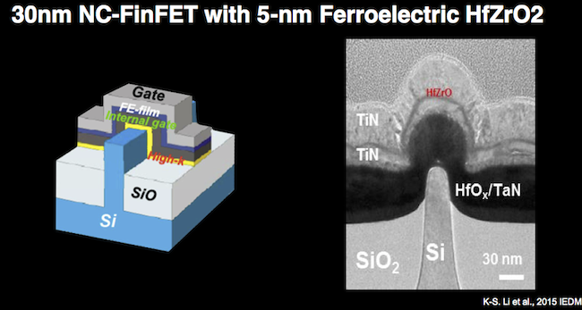
Diagram and SEM image of the NC-FinFET (UC-Berkeley, et al)
The negative capacitance aspects of the device were developed by Hu’s joint lead in the new research group, Associate Professor Sayeef Salahuddin, also based at UC Berkeley.
Other attractions in the proposed NC-FinFET structure include thorough compatibility with CMOS processes, as evidenced by the use of Hafnium Zirconium Oxide (HfZrO2) for the ferroelectric film. This material is already, as Professor Hu said, “familiar to manufacturing”.
Professor Hu acknowledged that the NC-FinFET is just one of a number of competing next-generation technologies. Rivals include stacked 2D circuits, ultra-thin-body FETs (possibly leveraging FD-SOI technology), tunnel transistors and others based on III-V materials. His main theme during his SNUG presentation was the need for research to continue on all fronts: “The world needs us,” he said.
Post finFET funding challenges
However, Professor Hu also sought to highlight increasing challenges in funding research and other programs that advance the broad semiconductor industry along a Moore’s Law-based performance path.
In addition to the NC-FinFET work, his department at UC Berkeley is also responsible for ongoing development of the BSIM Compact Model, the leading family of SPICE models for IC simulation and one that, to date, has been distributed under an open-source license.
However, there is still a cost. Professor Hu said that the finFET and FD-SOI standard process models required 11 man-years of work by six PhD students and seven post-doctorates.
“The work depends on the goodwill of companies in the industry but some, such as TI [Texas Instruments] and IBM have recently exited the area,” Professor Hu said.
New backers – including Synopsys and Silvaco in the EDA space – have stepped up to fill the resulting shortfall. But more are needed – not just in EDA but also the IP and fabless sectors – for the BSIM modeling work to continue and then be made available to the industry as a whole.
