GaN power makes progress at IEDM 2015
With III-V devices possibly supplanting silicon in future logic-oriented processes, gallium nitride (GaN) could be an important material for the power devices that sit alongside SoCs or, potentially, even on the same die.
GaN so far has been developed as a planar technology for both logic and power processes. That is because GaN, like gallium arsenide, is difficult to handle in manufacturing: the material generally needs to be deposited onto a carrier wafer. That used to be sapphire but for cost reasons and to take advantage of much larger wafers, process developers have used strain-relief techniques to allow GaN to sit on top of regular silicon.
The result is that, unlike silicon carbide (SiC), GaN does not readily suit the type of vertical structure that is useful in high-current power-switching designs because it improves the density of parallel transistors. However, in a paper for IEDM 2015, Daisuke Ueda of the Kyoto Institute of Technology argued drift-region resistance is more important in high-voltage devices than channel resistance, which helps planar devices as much as vertical.
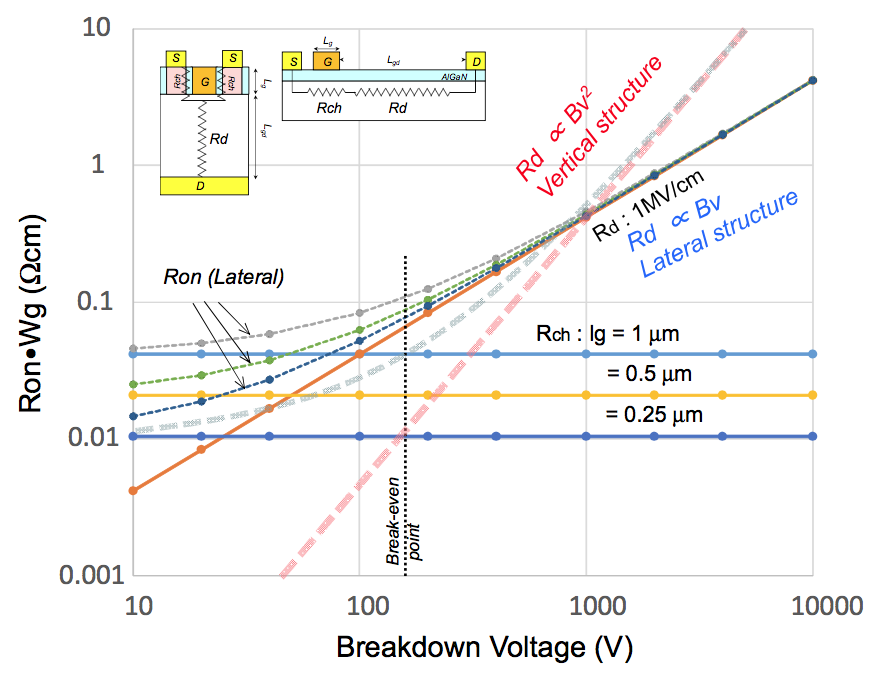
Image Impact of drift and channel resistance on planar and vertical transistors (Source: Ueda)
The vertical structure though also eases metallisation as the power-handling contacts are made to different sides of the wafer and spreads out heat generation. Because it is readily compatible with vertical structures, SiC has tended to edge GaN out as a high-power, high breakdown-voltage technology, with the III-V material looking better today as an RF-capable technology. Several papers at IEDM described work intended to overturn that notion.
Tetsu Kachi described work at Toyota Central R&D Labs to develop vertical structures, one based on a depletion-mode DMOS device and the other on a form of trench FET that employs a novel etching process. Conventional dry etching forms a V-shaped trench with undesirably rough edges. Further wet etching produced widened the trench and not only formed a much smoother surface but flatter sides and bottom – aligned with the crystal orientation of the GaN substrate.
A key problem remains forming the GaN substrate itself. Techniques are now producing a high-quality crystal. Impurities still cause dislocations but they are no longer propagating to the epitaxial layers, allowing low-leakage devices to be formed. But making wafers with uniformly high quality remains a challenge, according to Kachi.
MIT researchers took an alternative approach to the vertical device by developing a novel structure that allows vertical conduction with a silicon substrate. However, the current flow is not designed to pass right through the substrate to a bottom contact. Instead, the current flows vertically to a lower contact that still sits on top of the silicon/GaN buffer layers. The team led by Tomás Palacios has made diodes using a vertical silicon nitride nano-ribbon but has found leakage to be too high. Sidewall leakage appears to be the main problem, so the team has worked on better surface treatments. Although the vertical topology may not be ideal for discrete power devices, the MIT team sees the approach as good for integrating power with silicon logic.
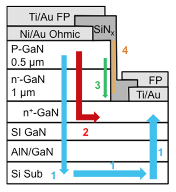
Image Leakage paths in MIT vertical GaN-on-Si diode
According to Ueda, GaN could have a bright future as a low-voltage, high-current power switching technology. The lack of a requirement for high blocking voltage supports miniaturisation and GaN transistors could be made much smaller – as much as 40 times smaller – than those possible with comparable silicon devices. However, as the structures get smaller, whether in a planar or vertical device, contact resistance in the source and drain regions reduces the power efficiency.
Ueda described a regrowth technique coupled with heavy germanium doping to improve the conductivity of the source and drain – increasing carrier concentration by an order of magnitude.
As GaN becomes more common in power converters, electromagnetic compatibility could be an issue especially if the technology does take hold in low-voltage, high-current designs close to processors and FPGAs. The high switching frequency possible at high efficiency with GaN will cause parasitic stray inductances that not only result in interference but could cause gate voltage overshoot that goes as far as to kill the device itself. Researchers from CEA said new topologies will be needed as well as the use of copackaging technologies to reduce the inductance of wiring between the power transistors and load capacitors.
The better conductance of normally on GaN transistors compared to their normally off counterparts will also call for topology changes. That, according to CEA, could lead to the use of ‘cold startup’ circuits that act as front-ends to the more familiar H-bridge converters.
