Shape a major choice for sub-10nm nanowire FETs
Using the results of simulations with the company’s Garand TCAD tool, Gold Standard Simulations (GSS) says nanowire transistors look practical down to 5nm but that designers need to carefully explore how the wires are shaped as quantum confinement and quasi-ballistic effects take hold.
In a blog post at the GSS site, the company shows a number of results for different nanowire cross-sections that show, even in a fully circular nanowire, electrons split into at least two narrow paths. A square profile with the same cross-sectional area appears to provide a greater capacity for electron transport but that is beaten by a flattened ellipse in the published diagrams.
In nanowire transistors, circular and elliptical profiles are possible because the gate will be wrapped fully around the channel material, in contrast to the three-sided encapsulation of a finFET. In principle, drive current can be increased through confinement-induced band splitting, which adds a further dimension for process, material and nanowire shape choices. Conceptually similar to a finFET, multiple nanowires can run through the same transistor to further increase drive current.
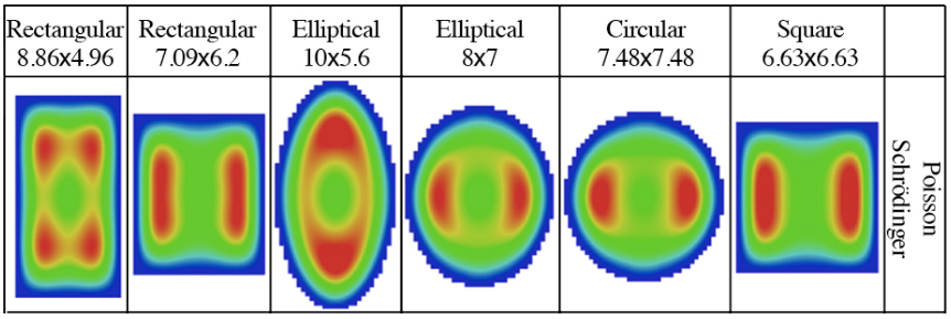
Image Charge distribution for various nanowire shapes of the same cross-sectional area
As with finFETs and FD-SOI devices, dopant effects and the increasingly problematic roughness of gate and nanowire edges, as well as metal gate granularity will affect carrier transport and introduce significant variability.
The interactions between these effects will make predictive TCAD vital, GSS said. The company has built algorithms to predict quantum mechanical and non-equilibrium transport effects as well as global and local variability effects into the Garand tool. An additional ensemble Monte Carlo transport, which can perform multiple Monte Carlo runs on different sub-bands, is designed to handle the simulation of different channel materials, such as III-V and germanium that chipmakers expect to use to increase overall mobility.
Professor Asen Asenov, GSS CEO, said early simulation should speed up process development for such small devices significantly. He added: “It can also help fabless companies to make the right technology choices for their products in the diversified-technology world where [nanowire transistor] technology will compete with conventional bulk, FDSOI and FinFET CMOS. Once the choice is made the technology can be optimised for the requirements of data farms, laptops, tablets, smart phones, wearable electronic devices, and the IoT as a whole.”
