Mentor unites chip-to-package flow with Xpedition Package Integrator
Mentor Graphics’ decision to launch an integrated chip-to-board-to-package flow based around its Xpedition tools – but also pulling on many others – should not come as much of a surprise, as it addresses the latest stages for design complexity highlighted by the move to 3D chip stacks and denser PCBs generally.
Mentor has also been extending Xpedition’s reach and deepening its integration for about a year, since a relaunch and rebranding in Spring 2104.
The Xpedition Package Integrator (XPI), launched today (March 23) after a solid run-in with Tier One customers, acknowledges what most designers already know: you can no longer treat chip, board and package design as entirely separate activities, particularly for interposers and stacked die.
More important is that XPI looks to take the market beyond the ad hoc way in which some of those boundaries have been overcome using ‘raw’ data in Excel spreadsheets or fudges that enable communication between different tools and database types. Rather it aims to offer a path from chip to package within a single environment.
Mentor’s claimed functionality for XPI gives a good idea of the tasks that it seeks to integrate:
- Single tool, cross-domain integration platform (EDA tool neutral, aggregates existing flows)
- Multi-view connectivity management
- Targeting multiple board form-factors (platforms)
- Rule-driven, smart pin planning and optimization
- System visualization and optimization
- Streamlined and automated library development
- Prototype to production flow (pathfinding)
- Single physical layout solution
- Electrical and thermal characterization
There’s a lot to take in there at one go, but you can immediately see how XPI is also drawing on the existing HyperLynx (analysis/verification), Valor (production), Nimbic (electromagnetic simulation) and FloTHERM (thermal analysis) tools. Perhaps that becomes clearer in this graphical representation of XPI.
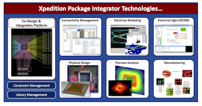
The Xpedition Package Integrator Suite (Source: Mentor Graphics)
Xpedition Package Integrator goes across the flow
The goal is multi-level, multi-challenge, across-the-board optimization in the face of rising pin-counts, burgeoning design layers, building cost pressures (particularly due to the Internet of Things) and the blurring of design competences.
That last challenge is particularly interesting today given how die-stacking and interposers have opened up a knowledge gap between the roles of foundries and OSATs that both sides have been battling to fill.
However, one particular innovation of note – the introduction of more detailed ‘virtual die models’ within XPI – then also addresses the boundary between chip and board design.
“The historical die models no longer cut it for chip-to-package flows. First, the board and package designers need more information: More about the IP blocks, how they are positioned; more about layer routing; more about the die bumps and so on,” says Dave Wiens, business development management for Mentor’s System Design Division.
“But you don’t just want to say, ‘Here’s the chip’. You want to be able to feed ECOs bi-directionally, to feed those back to the layout team working on the chip. And we’ve now added that.”
As noted, Xpedition Package Integrator is available immediately. With it having put so much on the table at one go, we will be taking a deeper dive into its use and its capabilities this week and next in a couple of more task-specific technical articles.
