CEA-Leti deals with heat issue on monolithic 3DIC
At IEDM 2014, CEA-Leti presented a technique that could help lead to practical monolithic 3DIC designs. Using these and other techniques in development, the research institute says fabless companies could start to trial the technology within a couple of years.
A key problem with making monolithic 3DICs is the thermal budget of the base-layer transistors during manufacture. The wafer and chip bonding techniques used for through-silicon vias on the current mainstream 3DIC technology operate at a much lower temperature than those needed for monolithic 3DIC.
CEA-Leti’s approach does not demand the formation from scratch of high-quality epitaxial silicon on top of the base layer of transistors. The research institute uses layer transfer similar to that needed for the silicon-on-insulator (SOI) developed in collaboration with STMicroelectronics. However, the transistors need to be further processed and annealed at high temperature to ensure they operate at peak efficiency. The additional heat can damage the layers underneath.
Resistance problems
The bulk of the problem is concentrated in the silicide used to form a contact between the gate and surrounding circuitry. Maud Vinet, CEA-Leti’s manager for advanced CMOS processes, said: “It does not lead to dysfunctional transistors. You start by losing performance, through morphological degradation that increases the access resistance.”
The technique described by CEA-Leti at IEDM to avoid damaging the silicide is to combine laser annealing – which focuses energy on the areas of the wafer needing heat – with a capping layer made from silicon nitride in the experiments to stop heat from leaking through.
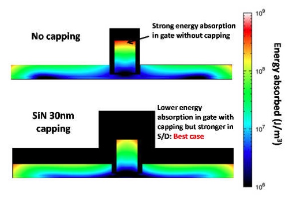
Image CEA-Leti's capping layer distributes heat from laser annealing more effectively
“The main idea behind the capping layer is that it protects the gate,” said Vinet. But there is an additional benefit to the layer. It can be used to activate dopants in the source and drain regions because it tends to spread the heat from annealing laterally as it moves down through the wafer.
Dealing with throughput
A possible roadblock to adoption is the speed of laser annealing, which is much slower today than the bulk heating methods generally used. “The lasers we are working with at the moment, which operate in the 300nm UV range, they are R&D lasers. We are working with suppliers to find something that is more compatible with throughput. It’s a challenge but we are working on it, to make sure that laser annealing can meet the requirements.
“We are trying to optimize the energy transfer to be as fast as possible – increasing the number of pulses per second,” Vinet added, noting that the issue at the moment is the recovery time that the current generation of lasers require. “There are some physics and technological development to be done so we can make sure everything is efficient and make sure the tool has less downtime.”
The CEA-Leti team found a 30nm-thick silicon nitride layer most effective at distributing heat and ensuring that the temperature of the lower layer does not exceed a target of 600°C. This could be pushed further, down to 500°C using additional porous materials for their low thermal conductivity or even materials that act as a reflector for the heat.
Routing performance
As well as working on the manufacturability of monolithic 3DICs, CEA-Leti is looking at design and routing issues. Potentially, bringing transistors closer together can reduce overall interconnect delays and reduce power for mobile designs, which is something that a recent paper by Qualcomm has suggested.
To help improve performance, the team is looking at low-resistivity interconnect options, with tungsten possibly returning as an important material and potentially displacing copper in some areas.
“Tungsten becomes better than copper on narrow lines,” Vinet said.
The main issue with tungsten is the barrier layer need to prevent tungsten diffusing into surrounding regions and damaging them. Improvements to the tungsten-deposition process could remove this high-resistance barrier. Another possible material candidate, Vinet said, is cobalt.
Design’s influence
A key question is whether 3DIC will be restricted to a single additional layer, providing a one-generation boost to Moore’s Law, or can support multiple upper layers. In principle, FD-SOI architectures could support more than one layer readily. Vinet said designs with up to four layers look to be manufacturable. The determinant, however, will be design, she said.
Design styles, such as whether different layers will contain complementary transistors for the same standard cells or completely different cells, will control the degree to which chipmakers can make use of the additional active layers.
Vinet said the work is progressing well enough to think about taking designs from fabless companies in the near future. “Our ambition is to start to receive layouts from fabless companies in 2017. The world is beginning to think monolithic 3D is a very interesting and promising technology. It is a very straightforward way to go and doesn’t need a lot of innovation.”
