From Darwin to Mao: how multi-patterning could move up the flow
We have heard a lot about patterning in terms of advanced process nodes. But it has largely been confined to what happens after a design has gone to the fab. Could patterns be about to have greater, even radical influence higher up the design flow?
Making lithography work requires a myriad of techniques, and things are not going to get any easier as we go beyond the 14/16/20nm planar/finFET band. Imagine also that there’s no EUV – it isn’t hard to do.
Joe Sawicki, vice president and general manager of Mentor Graphics Design-to-Silicon division, is one of the industry’s ‘go to’ guys on all things DFM. If the Calibre family is your brand, that’s a given.
Earlier this year, Sawicki mapped out some of what he sees as the challenges ahead and the techniques that will address them for an audience of optics specialists.
As important as many of these are – inverse lithography, negative resist, pixel-by-pixel light source optimization – the detail of making them work falls into the ‘invisible’ category for those outside that original audience. Even to foundry and DFM specialists they often fall into what Sawicki calls the ‘good juju’ category – bits of magic that an EDA tool accomplishes behind the scenes so the user doesn’t really have to worry about them. Well, not that much.
But Sawicki also described an emerging continuum that charts the influence of patterns from ‘evolution to revolution’ – or ‘Darwin to Mao’. Its implications could force us to rethink far more than the manufacturing process.
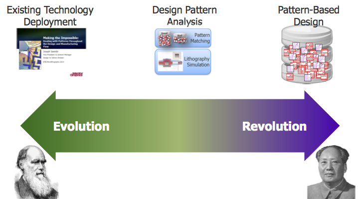
Figure 1 From Darwin to Mao - disruptive patterns (Source: Mentor Graphics/SPIE Microlithography 2014)
The thing to look at is, as you might expect, the far right of that continuum: ‘pattern-based design’. If it becomes a necessary part of future chip design, the concept could negate a chunk of the intellectual capital invested in a traditional flow.
Patterns? You want me to do WHAT?
“I’ve got a base level cell. In custom it’s my PCell, in digital it’s a standard cell that someone else designed. And I take them, place them and connect them,” Sawicki says.
“As a custom designer, I can live with the fact that, say, I get only so many shapes to build my transistor, and I’ve been working with restricted design rules for a while. For placement, I can live with the fact that I can only place things in certain relationships to each other. And I connect them up with wires.
“‘OK, so now you want me to use these ‘patterns’. What are these? Patterns that connect, you say. Well, that’s just weird.’”
As Sawicki notes, we have spent the last 50 years or so doing things very differently, refining the process all the time: “Our entire infrastructure is based around taking hundreds of billions of placements and connecting them together in a timing-closed manner that relies upon algorithms that look at channels or a grid: ‘Now you want me to use patterns – now you want me to throw all that out the door?’”
Given that, why should patterns move up the flow? Why should we even allow it?
One important factor is that pattern matching is already helping chip manufacturers. Both Samsung and GlobalFoundries have gone public on their use of the technique.
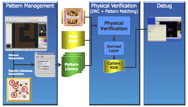
Figure 2 Figure 2. A Pattern Matching flow (Source: Mentor Graphics/SPIE Microlithography 2014)
There are good reasons why the fabs have adopted pattern matching. The impact of double (and multi) patterning in terms of printing a device have been major drivers. As another example, when working across multiple layers during manufacturing, the fabs are now at a point where a big issue can be reflectivity of the light source back from a lower layer to one above it. They moved from 2D to 3D thinking before finFETs hit the agenda.
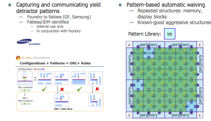
Figure 3 The benefits of pattern matching (Source Mentor Graphics/SPIE Microlithography 2014)
Having started pattern matching, there is now a trend towards using related test not just to throw away bad parts but, says Sawicki, “to take a production chip and turn it into a constant test chip for your process.” Scan test techniques and structural analysis help to create a useful feedback loop.
“You can do diagnostics. So, if I get three errors at a certain point and I always get these three bits not working, I’ve just learned something. If I cast back the cone of logic that’s connected to all this, I’ve found out that there’s some bad logic in there. It’s a simple enough concept but it gets more and more complex. We call that Layout-Aware Diagnostics and we’ve got customers doing this now,” says Sawicki.
But you can go further.
Big Data in a cultural revolution
“You take this basic capability but then you collect lots and lots of data. You see something, you take it to physical analysis. Then you start statistical analysis. You’ve got all this failure data highlighting all these failure suspects in these designs. So you ask, ‘If I look at my via layer failures, do any have a higher rate of failure that I would expect based on their simple predominance in the design?’” says Sawicki.
“Then it starts. You get…. Pop! Via 6 is not working; it’s failing at six times the rate. Pop! This pattern isn’t working; it’s failing at a higher rate than any other pattern that looks like it.”
At the foundry level, this kind of data can be tied back to, say, misalignment in a pellicle, tweaks needed to CMP, and so on. But, what about the ‘revolution’?
“So, this is your Mao. People are beginning to say why don’t we just invert this. We also know that we can make these patterns. So we won’t give you design rules, we’ll just say, ‘Just use those patterns in your design’. That’s a pretty huge change,” Sawicki notes.
“But there’s also a middle way. As a foundry, you can say, ‘I print chips and I can do pattern decomposition of those chips, which will give me a library that says I’ve done these things and they did or did not work.’ You then allow designers to compare their work against that to see if everything they’ve done has been done before successfully. And they use that to make any adjustments before you send over the files.”
For now, all this is some way from deployment in its entirety though it is being discussed. Mentor has customers using some of the techniques that would be part of such a flow. No-one, however, has pulled all of them together at even the foundry level. Yet.
“And the patterns themselves are a challenge because of the number of them. There are hundreds of millions that are used less than 10 times, so many independent ones that it’s not even funny. Then, there are very few – less than 10 – that are used a lot in design,” says Sawicki. “So there are practical limits to the analysis.”
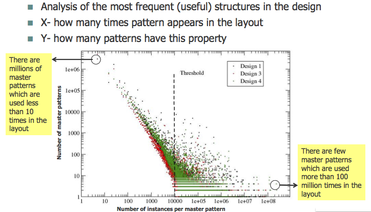
Figure 4 Library contents for printable patterns (Source: MG/SPIE)
Consider the graph directly above. “If you look at the graph, you can say that maybe some of those patterns are not the same but close enough that you can collapse the data,” says Sawicki. “But that’s still a hard one —once you start doing this, you ask have to ask yourself, ‘When might I be doing something that I don’t know is wrong?’
“Still, there are some very smart people who do think we can make this work.”
Sawicki himself thinks that the future will be a mixture: “We’ll take a bit of this, a bit of that and maybe a lot of this. But there is a sociological as well as technological problem. Do you realistically want to retrain the whole industry? Good luck with that.
“But, it just says again that there are no easy solutions here.”
