Minimal 32bit IP cores tackle connected devices market
Cortus has launched two 32bit soft processor IP cores for the “connected intelligent devices” market, a phrase it uses to highlight its belief that there is more to the current Internet of Things hype than just Things connected to the Internet.
“We’re avoiding the IoT buzzword,” said Roddy Urquhart, vice president of sales and marketing at Cortus. “The same constraints apply whether you’re connected to the Internet or not.”
Does the market need another soft processor core? Cortus argues that the IoT marks a third wave in the development of mass computing, whose first wave was defined by the PC market and whose second by mobile computing. The market for connected intelligent devices, it argues, will be so diverse that there will be room for many more architectures.
“The rules are going to change again for this new wave of devices,” said Urquhart. Designs will be particularly constrained by cost, and often by power consumption, calling for minimalist cores that can do just enough to satisfy a basic function, such as running a Bluetooth LE wireless stack.
New instruction set
To that end, Cortus has introduced a second version (v2) of its instruction set, in a bid to increase firmware code density and hence reduce on-chip memory requirements.
“Five years ago, embedded SoC designers cared about area and power,” said Urquhart. “Now they are also concerned about the size of memory necessary to support the firmware. So we’re trying to balance the core size and the code memory size.”
The v2 instruction set adds 24bit instructions to the 16- and 32bit instructions of the v1 set. Urquhart says that on a wide set of benchmarks, the v2 instruction set can achieve an average 16% denser code than the v1 version, at the cost of a 12% bigger core. Cortus says that, dependent on the type of memory being used and the technology in which it is built, it is worth moving to the v2 cores when the code memory reaches about 64Kbyte.
Cortus says it will keep offering products based on the v1 instruction set, and that any C/C++ or assembler code developed for the v1 cores can be run unmodified on the v2 cores.
The IP cores
The APS23 core is designed for in systems that are always on/always listening systems and those with less demanding clock frequencies, such as Bluetooth Smart.
It has a Harvard architecture, sixteen 32bit registers, a three-stage pipeline and a sequential multiplier. It supports the AXI4-Lite bus as well as Cortus APS peripherals.
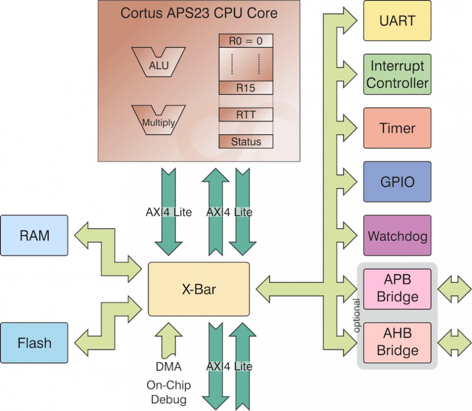
Figure 1 The Cortus APS23 core is designed to offer minimal services for always on/always listening systems (Source: Cortus)
The minimal usable APS23 CPU is about 9.8kgate when optimised for area. Dynamic power is 12uW/MHz on a 90nm process.
The maximum clock speed of the core is 200MHz on the same 90m process, from a 11.4Kgate core.
The APS25 core is approximately twice the gate count of the APS23. It has a Harvard architecture, sixteen 32bit registers, a five-stage pipeline, a pipelined parallel multiplier and a hardware divider. There’s parameterisable instruction and/or data cache support, as well as support for the AXI4 bus and Cortus APS peripherals.
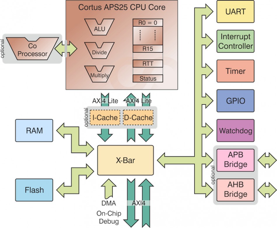
Figure 2 The Cortus APS25 is a more complex core with a deeper pipeline and coprocessor interface (Source: Cortus)
A coprocessor interface enables designers to add up to eight coprocessors to each APS25 core. Up to 4096 coprocessor instructions can be defined, and they can take two operands from the APS25 core and return a result back to it. These instructions can be inserted into C-code as function calls.
The APS25 can also support symmetric multiprocessing operations e.g. on dual or quad cores, to provide extra computational performance.
Minimum size of the APS25 is 18kgate, offering a 100MHz clock and 19.3uW/MHz power consumption on a 90nm process.
Maximum clock speed is 344MHz from a 25.4kgate design drawing 20.8uW/MHz on the same process.
Security
Urquhart argues that the small size of the cores and the coprocessor interface will make them a good basis for securing connected devices.
“The more you connect things together, the more you increase the attack surface for hackers to do something malicious,” he said.
Blackberry subsidiary Certicom has already used the coprocessor interface as a way of accessing a hardware accelerator for the key Galois field multiplication algorithms used in elliptical curve cryptography.
Under special licensing conditions, some customers have also been given rights to modify earlier versions of the core, for example by adding functions such as secure random number generators and secure clocking schemes.
Urquhart also argues that because the new cores are so small, it makes it easier to improve chip security by running two cores in parallel, but offset by a clock cycle. This means that any fault injection attack, such as disturbing its power supplies, buses or clock network will cause different faults in the two cores, which would otherwise return the same results, albeit offset by a clock cycle.
