IoT mixed signal design: keep everything in the green
A webinar organized by ARM and Cadence Design Systems shows how the system-level and implementation-level representations of a mixed-signal design can be linked together and kept in sync as the project progresses, making it easier to tune firmware and analog electronics together. The companies see this kind of flow as being particularly useful for a new crop of internet of things (IoT) applications where there is likely to be a strong interaction between software and sensor data.
Diya Soubra, CPU product manager for Cortex-M3 processors, said ARM has put together a design kit for the Cortex-M0, the small low-power processor that the company has aimed at IoT-type applications. The kit includes the RTL and models for the core as well as a number of commonly used peripherals as well as the infrastructure for adding custom mixed-signal blocks to the ARM peripheral bus (APB). Typically, the interface will use a register defined in the APB address space that can mapped across to the firmware development environment as well as the hardware design.
Once the basic connections are setup, the firmware development can be tied into the rest of the design flow, which was demonstrated through the specification and design of an IoT pressure regulator.
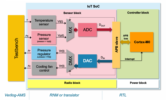
Image Block diagram of the regulator used in the demonstration
A further element in the design kit is an interrupt controller that remains active most of the time and which is used to trigger activation of the M0 core when a reading needs to be taken. “You can layer on software that is written to be low power-aware from the start so that it is not all idle while[…until] loops but software based on event-driven operation. From that you can get a dramatic power reduction,” said Soubra.
System-level descriptions
Using those hardware building blocks, the presenters proposed a mixed-signal flow that combines tools from both ARM and Cadence from the system down to the implementation level.
Ian Dennison, solutions senior group director of the custom IC and PCB groups at Cadence, explained how the approach would be used in the context of the pressure controller: “To minimize power needs, once pressure in the pipe has been stablished, the sensor will power down. If the pipe gains or loses pressure, the sensor node will wake up again.”
The DAC used to control the valve actuator would be designed to sit on a different power island to that of the sensor ADC so that it would only need to be powered up to send a new setting.
Validating the system therefore meant the simulation of power states, firmware, and analog behavior before moving onto implementation. Rather than simulate the analog section using SPICE, which would dramatically increase simulation time compared to a digital-only hardware-software coverification environment, Dennison proposed the use of real-number modeling, a facility in SystemVerilog and similar languages that allows analog values to be manipulated. Based on a discrete-time approach, real-number models are significantly faster than continuous-time approaches such those used in SPICE although they sacrifice a level of accuracy.
However, instead of demanding that analog engineers write behavior from scratch using SystemVerilog, he proposed using a tool – SMG – that assembles analogue models from a schematic. This is not a full circuit schematic but a conceptual representation of the analog behavior that engineers assemble, pulling building blocks from a library of a hundred or so. “These building blocks cover a wide range of functions. For our DAC, we were lucky as we were able to use a block straight out of the library,” Dennison said. “The graphical approach has been much more popular. It’s a lot easier for the Virtuoso user to visualize rather than trying to build the same model down to the [SystemVerilog] statement level.”
Wiring the DAC block into the overall system involved providing the environment with a register definition, which could be used by the ARM SDK tools to support firmware creation.
“Once we have the whole system model assembled we can start to worry about the system’s performance,” Dennison said.
Performance testing
Using the real-number model coupled to the firmware running on a processor model, the team could see how the code handled changes in input. The elements were coupled together in the Analog Design Environment, into which were fed key performance parameters that are displayed in spreadsheet form. “What we are seeking to do is get a green signal for each of the measurements to show that the design is in spec,” Dennison said. “If you have a processor in the design, you have the opportunity to move some of the calibration, for example, into firmware. With these elements in a tight loop, you can simulate all three at once: analog, digital and software.”
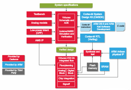
Image The ARM-Cadence mixed-signal flow
Once the system simulation performs as expected, the next step is to swap out some of the models and replace them with real circuitry, with the environment being used to check that the implementation marries with assumptions made during system-level simulation. “This time we create the sensor block from scratch using transistors. In the analog environment at the back we can size the design, work out the right length, finger count and width for the devices – all of the important parameters that will keep the elements in the spreadsheet still showing green. Once we have demonstrated that the design is still in spec, we can use the schematic to drive the layout tool using connectivity and constraint-driven techniques.
“We can use modgens to automatically create high-density transistor blocks. And use electrically aware design to ensure that the physical wires can carry the current without IR-drop problems,” Dennison added. “Then we can do a lot more performance analysis in the Analog Design Environment, to see if we can improve the power shutoff current levels or reduce parasitics.”
Correlating results
The simulation does not need to be tied to the physical implementation beyond this point. The runtime difference makes further software development difficult – 54 minutes versus less than half a second for a typical operation. The results of the transistor-level simulation can be tied back to the system-level representation, elaborating the model to better show the circuit response to stimuli.
“You can set tolerances and create a regression environment. If anyone is tweaking at the transistor or behavioural level, you can see if the green lines turn red,” said Dennison, alerting designers to a potential mismatch. “What we are trying to do is keep these things in sync.”
Once the system and analog design are ready, the process can then move to digital implementation and chip assembly. The webinar is available at Cadence’s site.
