FinFETs’ III-V future promises sub-7nm, RF and opto CMOS
FinFETs for 7nm and below processes will be able to integrate high-mobility III-V materials despite being built on silicon processes, thanks to recent work by imec.
The Leuven-based nanoelectronics research centre has managed to grow InGaAs and InP materials epitaxially on 300mm silicon wafers, using the layers to selectively replace part of the silicon fin.
One problem with growing such layers on silicon is the mismatch between their crystal structures. This causes tension at the interface of the materials, which in turn causes defects that can run into the upper layer of the compound semiconductor – for example, into the active part of a transistor channel.
One way to address the lattice mismatch issue is to alloy the guest material with silicon, and then use a series of layers of steadily changing material ratios to make the transition between the two lattice structures in a number of smaller steps. This works, but is slow and therefore costly in mass production.
Companies such as TSMC have experimented with ‘aspect-ratio trapping’ to solve the same problem. This means growing the guest material in deep, narrow (i.e. high aspect-ratio) trenches, so that any threading dislocations caused by the lattice mismatch terminate at the trench wall rather than running up into the active area of the material.
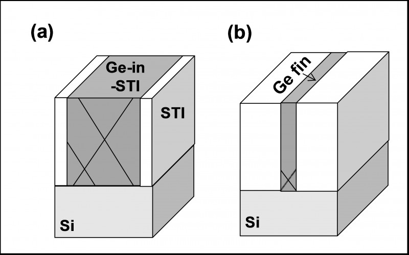
Figure 1 A narrow, tall trench means that dislocations caused by lattice mismatches terminate at the trench walls before they can reach the active area of the device (Source: TSMC, IEDM 2012)
In imec’s latest work, part of the silicon fin is replaced by a layer of InGaAs on top of a layer of InP. An overall lattice mismatch of 8% is accommodated by a combination of the trench structure, aspect ratio trapping, and the use of the two III-V layers.
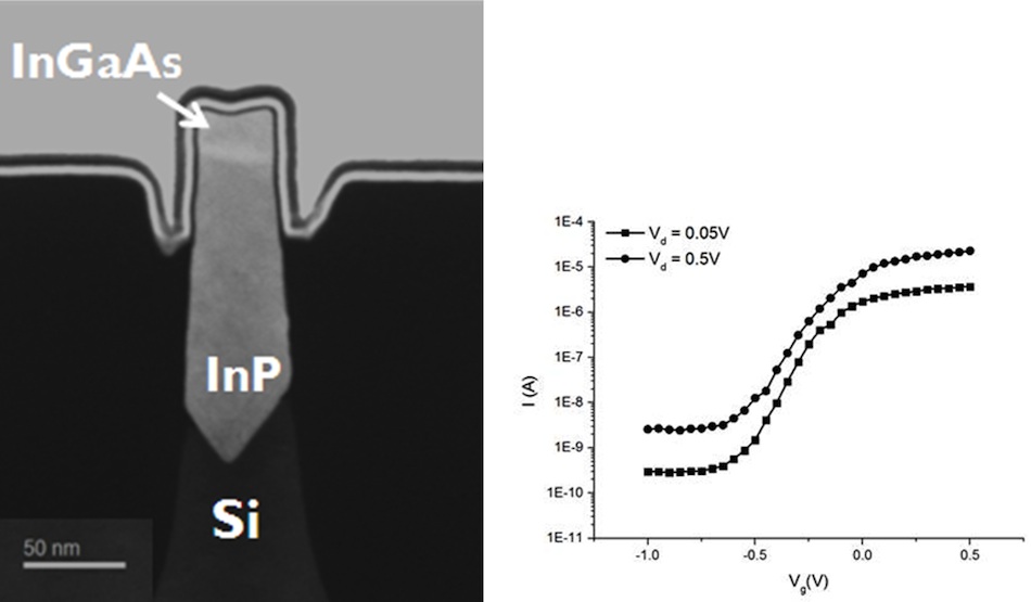
Figure 2 In this epitaxial integration of III-V materials onto the tip of a silicon finFET, the InP layer manages lattice mismatch and provides electrostatic confinement for the InGaAs channel (Source: imec)
According to Aaron Thean, director of imec’s advanced logic program, “the function of the InP is to create a buffer where defects are generated away from [the] InGaAs channel. Besides aspect ratio trapping, epitaxial-wise the choice of InP rather than InGaAs is important and it is part of the material and process innovations.”
More details of how this achieved will be covered in a future paper, according to Thean.
The InP layer also helps the device’s performance.
“The InP forms a quantum well with InGaAs, which improves electrostatic confinement in the channel,” he said. “However, it is lower in carrier mobility than InGaAs and so it’s not [used as] the channel of the device.”
The new process builds on a ‘classic’ finFET process, replacing part of the silicon fin and therefore inheriting its isolation characteristics.
According to Thean, the gate of this device runs down the side of the fin by as much as 50nm, defining the fin height.
“The gate runs past the InGaAs/InP heterointerface, which indicates that the electrostatic confinement is a combined effect of trigate action and quantum well isolation, which is expected to improve electrostatic control,” he said. For comparison, he added, a typical silicon fin or trigate is only about 30nm or so tall.
Imec argues that this work on heterogenous integration of III-V materials onto mainstream CMOS processes shows a way forward for CMOS processes beyond 7nm, as well as creating opportunities in hybrid CMOS-RF and CMOS optoelectronics.
The work has been carried out as part of imec’s core CMOS research program, whose partners include Intel, Samsung, TSMC, Globalfoundries, Micron, SK Hynix, Toshiba, Panasonic, Sony, Qualcomm, Altera, Fujitsu, nVidia, and Xilinx.
